Project 19: Calculator with 7-Segment Display
Combine FSM input, ALU, and multiplexed display for a calculator.
Quick Reference
| Attribute | Value |
|---|---|
| Difficulty | Advanced |
| Time Estimate | 2 weeks |
| Main Programming Language | Verilog (Alternatives: VHDL, SystemVerilog) |
| Alternative Programming Languages | VHDL, SystemVerilog |
| Coolness Level | High |
| Business Potential | Low |
| Prerequisites | FSMs, ALU, Debouncing |
| Key Topics | Input FSM, Datapath, Display multiplexing |
1. Learning Objectives
- Design a multi-stage input FSM
- Integrate ALU for operations
- Drive multiplexed 7-seg display
2. All Theory Needed (Per-Concept Breakdown)
Finite State Machine Design
Description/Expanded Explanation of the concept
FSMs model systems that move between discrete states. They are the backbone of controllers: traffic lights, vending machines, UARTs, and CPUs. A clear state diagram and correct next-state logic are essential.
Definitions & Key Terms
- State -> encoded system condition
- Moore FSM -> outputs depend only on state
- Mealy FSM -> outputs depend on state and inputs
Mental Model Diagram (ASCII)
S0 --in--> S1 --in--> S2
 ^                 |
 +-----------------+
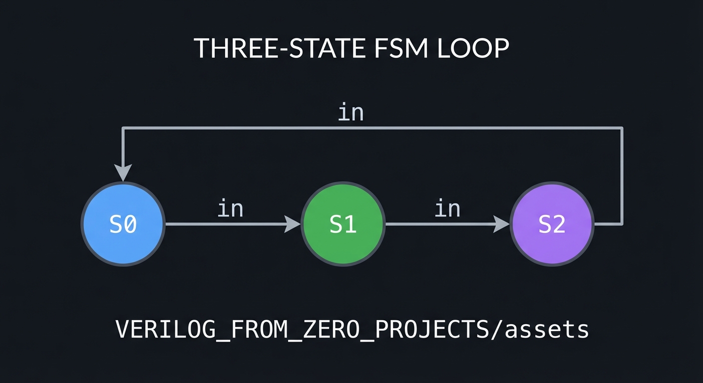
How It Works (Step-by-Step)
- Define states and transitions.
- Encode the states.
- Implement next-state combinational logic.
- Register the state on the clock edge.
Minimal Concrete Example
always @(posedge clk) begin
  if (reset) state <= IDLE;
  else state <= next_state;
end
Common Misconceptions
- “State encoding doesn’t matter.” -> It affects area and speed.
- “Mealy is always faster.” -> It can glitch if inputs change.
Check-Your-Understanding Questions
- When would you choose Moore over Mealy?
- How do you avoid glitches on outputs?
- How do you handle illegal states?
Where You’ll Apply It
- This project: used in Section 3.2 and Section 4
- Also used in: P11-traffic-light-controller.md, P13-serial-pattern-detector-finding-10110-in-a-bitstre.md, Final CPU
Datapaths and Flag Generation
Description/Expanded Explanation of the concept
A datapath is the collection of registers, muxes, and an ALU that moves and transforms data. Flags (zero, carry, negative) are simple but essential signals that let control logic make decisions.
Definitions & Key Terms
- Datapath -> the data-processing portion of a design
- Control -> logic that selects operations and routes data
- Flags -> status bits derived from results
Mental Model Diagram (ASCII)
[Regs] -> [ALU] -> [Regs]
          |  |
         Z  C flags
How It Works (Step-by-Step)
- Registers feed operands into the ALU.
- Control selects the ALU operation.
- Result and flags are computed in the same cycle.
- Flags are stored or forwarded for decision-making.
Minimal Concrete Example
assign z = (y == 0);
assign n = y[7];
Common Misconceptions
- “Flags are only for CPUs.” -> Many control systems use them too.
- “Flags don’t need testing.” -> They are part of the contract.
Check-Your-Understanding Questions
- When should the zero flag assert?
- How do you compute a negative flag for unsigned data?
- Why separate datapath and control?
Where You’ll Apply It
- This project: used in Section 3.2 and Section 4
- Also used in: P19-calculator-with-7-segment-display.md, Final CPU
Debouncing and Synchronizers
Description/Expanded Explanation of the concept
Mechanical buttons bounce: they produce multiple rapid transitions on a single press. Also, a button is asynchronous to your clock, so it can cause metastability. A synchronizer chain plus a stability counter creates a clean, single transition.
Definitions & Key Terms
- Bounce -> rapid oscillation at a switch transition
- Synchronizer -> chain of flip-flops to reduce metastability
- Stable window -> required time with no changes
Mental Model Diagram (ASCII)
raw_btn -> FF -> FF -> stable_counter -> clean_btn
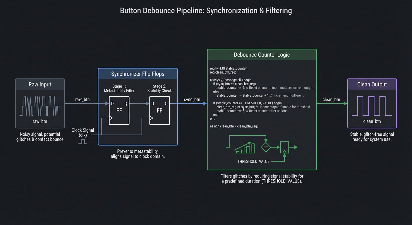
How It Works (Step-by-Step)
- Synchronize the raw input with two flip-flops.
- Count how long the input stays the same.
- Once stable for N cycles, update the clean signal.
Minimal Concrete Example
if (sync_btn == stable_btn) count <= 0;
else count <= count + 1;
Common Misconceptions
- “A button is just a logic input.” -> It is noisy and asynchronous.
- “One flip-flop is enough.” -> Two are standard for safety.
Check-Your-Understanding Questions
- Why is metastability a risk with buttons?
- What is the trade-off between stability time and responsiveness?
- Why not debounce in software on an FPGA-only design?
Where You’ll Apply It
- This project: used in Section 3.2 and Section 5
- Also used in: P19-calculator-with-7-segment-display.md, P20-pong-game-on-vga.md
3. Project Specification
3.1 What You Will Build
A calculator that reads button inputs and shows results on 7-seg displays.
3.2 Functional Requirements
- Requirement 1: Accept digits and operators
- Requirement 2: Compute results and display them
- Requirement 3: Debounce button inputs
3.3 Non-Functional Requirements
- Performance: Stable operation at the target clock and interfaces.
- Reliability: Deterministic outputs on all defined inputs.
- Usability: Clear ports and documented behavior.
3.4 Example Usage / Output
{p['example_usage']}
3.5 Data Formats / Schemas / Protocols
{p[‘data_format’]}
3.6 Edge Cases
- Overflow
- Divide by zero
3.7 Real World Outcome
3.7.1 How to Run (Copy/Paste)
vvp calc_tb
3.7.2 Golden Path Demo (Deterministic)
Run the demo command above with the provided testbench and confirm the outputs match the golden transcript.
3.7.3 CLI Transcript
Input: 12 + 34 =
Display: 46
3.7.4 Failure Demo (Expected)
# Example failure case
ERROR: Output mismatch at vector 3
Expected: 0x0A, Got: 0x0B
EXIT CODE: 1
Notes:
- Exit code 0 indicates all tests passed
- Exit code 1 indicates a test failure
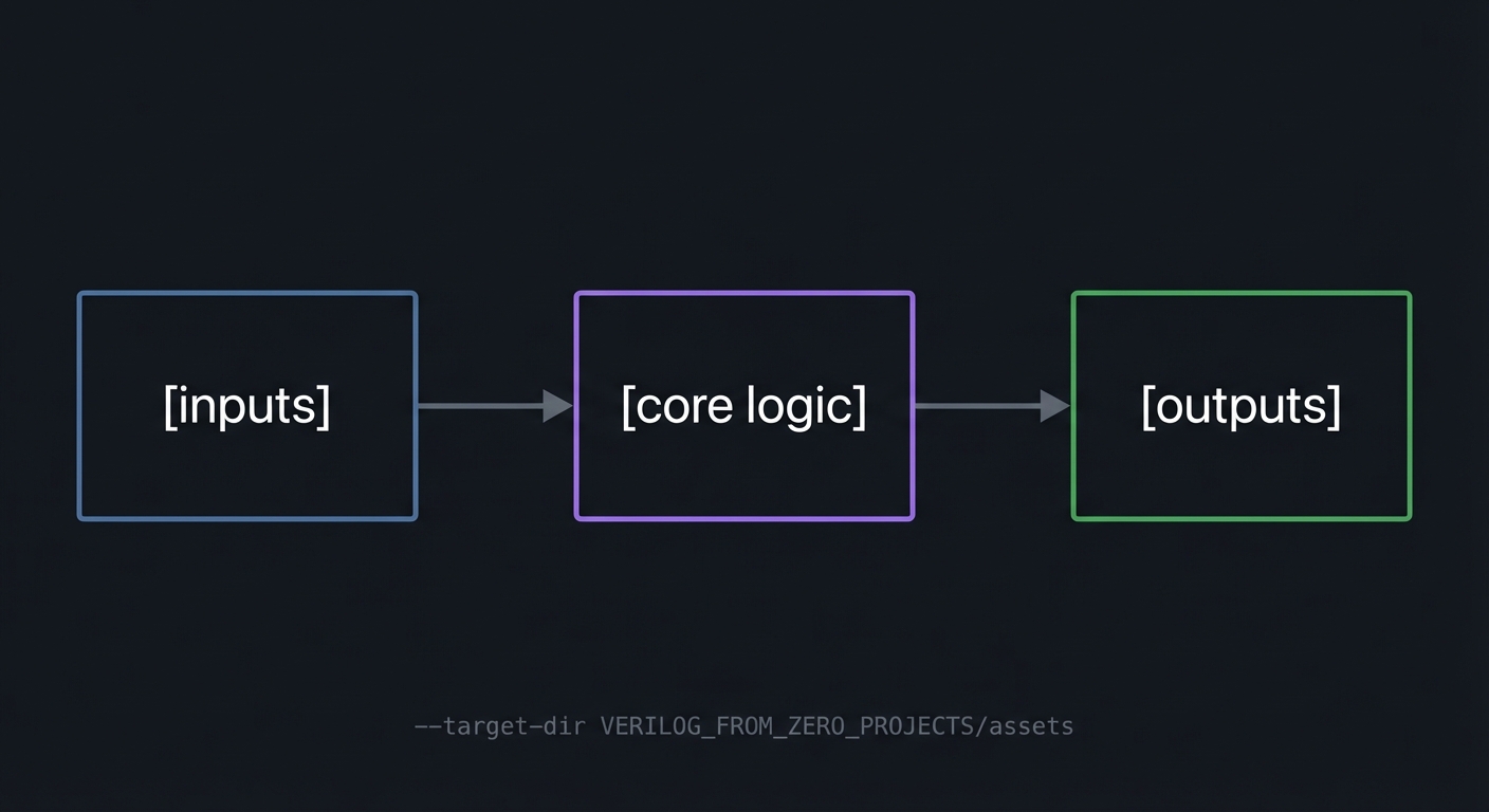
4. Solution Architecture
4.1 High-Level Design
[inputs] -> [core logic] -> [outputs]
4.2 Key Components
| Component | Responsibility |
|---|---|
| input_fsm | Digit/operator entry |
| alu | Performs operations |
| display_mux | Scans 7-seg digits |
4.3 Data Structures (No Full Code)
// Example signals (adapt to your design)
reg [7:0] state_reg;
reg [7:0] data_reg;
4.4 Algorithm Overview
Key Algorithm: Core control flow
- Initialize state/reset conditions.
- Apply inputs and compute outputs.
- Update state on clock edges (if sequential).
Complexity Analysis:
- Time: O(1) per cycle
- Space: O(N) for registers and logic
5. Implementation Guide
5.1 Development Environment Setup
iverilog -v
# Ensure GTKWave is installed for waveform viewing
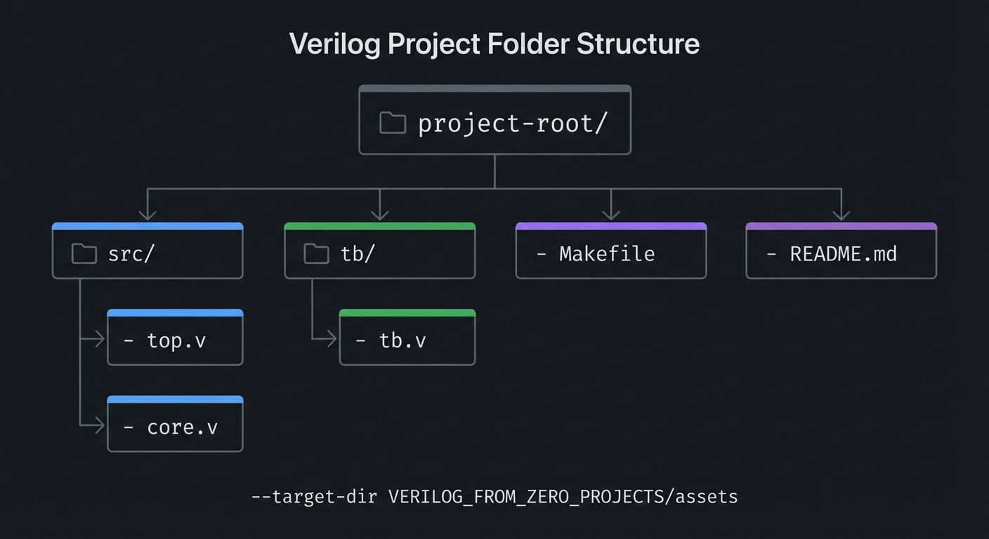
5.2 Project Structure
project-root/
|-- src/
|   |-- top.v
|   |-- core.v
|-- tb/
|   |-- tb.v
|-- Makefile
|-- README.md
5.3 The Core Question You’re Answering
“How do you combine input FSMs, datapath math, and display multiplexing?”
5.4 Concepts You Must Understand First
- FSMs
- ALU
- Debouncing
5.5 Questions to Guide Your Design
- How will you encode digits and operators?
- How many digits to support?
5.6 Thinking Exercise
Draw a state diagram for number -> op -> number -> equals.
5.7 The Interview Questions They’ll Ask
- How does multiplexing reduce pin count?
- Why debounce inputs?
5.8 Hints in Layers
- Start with single-digit operations.
- Add multi-digit support by shifting digits.
5.9 Books That Will Help
| Topic | Book | Chapter |
|---|---|---|
| Datapaths | Digital Design and Computer Architecture | Ch. 5 |
| FSMs | Digital Design and Computer Architecture | Ch. 3.4 |
5.10 Implementation Phases
Phase 1: Foundation
Goals:
- Establish core module structure
- Implement minimal behavior
Tasks:
- Scaffold module ports and internal signals
- Write a minimal testbench that compiles
Checkpoint: Simulation runs without errors
Phase 2: Core Functionality
Goals:
- Implement full logic
- Verify edge cases
Tasks:
- Complete core logic
- Add directed tests for edge cases
Checkpoint: All tests pass and waveforms match expectations
Phase 3: Polish & Edge Cases
Goals:
- Improve readability
- Document behavior
Tasks:
- Add comments and README notes
- Expand tests for unusual inputs
Checkpoint: Design is deterministic and documented
5.11 Key Implementation Decisions
| Decision | Options | Recommendation | Rationale |
|---|---|---|---|
| Reset strategy | Sync / Async | Sync | Simpler timing closure |
| Test coverage | Directed / Exhaustive | Exhaustive for small logic | Prevents missed cases |
6. Testing Strategy
6.1 Test Categories
| Category | Purpose | Examples |
|---|---|---|
| Unit Tests | Test core logic | Small vectors |
| Integration Tests | Test modules together | Full system |
| Edge Case Tests | Boundary conditions | Max/min values |
6.2 Critical Test Cases
- Test 1: Basic operations +,-,*,/
- Test 2: Debounce behavior for button press
6.3 Test Data
Use deterministic vectors and document expected outputs.
7. Common Pitfalls & Debugging
7.1 Frequent Mistakes
| Pitfall | Symptom | Solution |
|---|---|---|
| Display flicker | Scan rate too slow | Increase scan frequency |
7.2 Debugging Strategies
- Inspect waveforms at key internal signals
- Add temporary debug outputs to verify state
- Reduce testcases to the smallest failing case
7.3 Performance Traps
- Overly wide counters or combinational paths can reduce max clock
8. Extensions & Challenges
8.1 Beginner Extensions
- Add parameterization for widths
- Add optional features (enable, reset)
8.2 Intermediate Extensions
- Add configuration registers
- Build a simple driver or demo program
8.3 Advanced Extensions
- Integrate with another project in this series
- Implement a hardware demo on FPGA
9. Real-World Connections
9.1 Industry Applications
- Digital control systems and embedded peripherals
- FPGA prototyping and validation
9.2 Related Open Source Projects
- Yosys / nextpnr toolchain for open-source FPGA flow
- Example HDL projects in the FPGA community
9.3 Interview Relevance
- Demonstrates RTL thinking and verification skills
10. Resources
10.1 Essential Reading
- Digital Design and Computer Architecture - Focus on Ch. 5
- Digital Design and Computer Architecture - Focus on Ch. 3.4
10.2 Video Resources
- Search for project-specific HDL walkthroughs and waveforms
10.3 Tools & Documentation
- Icarus Verilog
- GTKWave
10.4 Related Projects in This Series
- See adjacent projects in
VERILOG_FROM_ZERO_PROJECTS/
11. Self-Assessment Checklist
11.1 Understanding
- I can explain the core concept without notes
- I can predict waveform behavior for basic inputs
11.2 Implementation
- All functional requirements are met
- All tests pass
- Edge cases are documented
11.3 Growth
- I can explain this project in an interview
- I documented at least one lesson learned
12. Submission / Completion Criteria
Minimum Viable Completion:
- Functional requirements implemented
- Testbench passes
- Waveforms inspected
Full Completion:
- All minimum criteria plus
- Edge cases covered and documented
Excellence (Going Above & Beyond):
- Hardware demo on FPGA
- Clear write-up of lessons learned
Appendix A: Deep Dive Walkthrough
A.1 Signal Map and Invariants
- Inputs:
clk,reset,btn[0..N](digits and ops) - Outputs:
seg[6:0],an[3:0](digit enables)
Invariant: Only one digit enable is active at a time during multiplexing.
A.2 FSM States (Suggested)
- ENTER_A -> OP_SELECT -> ENTER_B -> CALC -> SHOW
A.3 Deterministic Test Sequence
- Enter
1 2 + 3 4 =-> expect46. - Enter
9 * 9 =-> expect81. - Enter
5 - 8 =-> expect-3if signed mode supported.
A.4 Multiplexing Timing
- Scan rate: 1 kHz per digit (4 kHz total) for flicker-free output.
A.5 Debugging Tip
If digits flicker, increase scan frequency or ensure anodes are not overlapping.
13. Deep Dive Appendix
13.1 Timing and Resource Budget
- The keypad scan rate should be 1-5 kHz to feel responsive.
- Display multiplex should be > 1 kHz to avoid flicker.
- ALU operations are fast; the UI pipeline is the main timing challenge.
13.2 Waveform Interpretation Guide
- Watch scan_row, scan_col, and key_valid for key detection.
- Confirm digit_select rotates and segment data updates with it.
Example scan cycle:
row0 -> row1 -> row2 -> row3 (repeat)
13.3 Hardware Bring-Up Notes
- Use transistor drivers for 7-seg digits if current exceeds FPGA limits.
- Debounce keys in hardware or the FSM will see repeated digits.
- Use a slow step-through mode for debugging input logic.
13.4 Alternate Implementations and Trade-offs
- BCD datapath keeps digits separate and simplifies display.
- Binary datapath is simpler for ALU but needs conversion to BCD.
- Add stack-based operations (RPN) for a more advanced UI.
13.5 Additional Exercises
- Add memory registers (M+, M-, MR).
- Support negative numbers and sign display.
- Add decimal point and fixed-point math.