Learn Verilog: From Zero to Digital Design Mastery
Goal: Build the mental model of real hardware: signals that exist in parallel, state that advances on clock edges, and timing that can make or break a design. You will learn synthesizable Verilog (Verilog-2005 style RTL), interpret waveforms like a hardware engineer, and reason about clocks, resets, and metastability. By the end, you can design, simulate, and implement digital systems on FPGAs, integrate real-world protocols (UART, SPI, PWM, VGA), and explain why your designs work or fail. Your capstone is a small CPU you can single-step in simulation and run on real hardware.
Introduction
What is Verilog? Verilog is a hardware description language (HDL) for describing structure and behavior of digital circuits. You are not writing a sequential program; you are describing hardware that exists in parallel and reacts to signals. This guide focuses on the Verilog-2005 style RTL subset (widely supported by tools) and uses small, optional SystemVerilog features only inside testbenches when they reduce bugs.
What problem does it solve? It lets you design complex digital systems (ALUs, UARTs, VGA controllers, CPUs) without drawing every gate. Synthesis tools translate RTL into gates and flip-flops, and implementation tools map that netlist onto FPGA resources or ASIC cells.
Scope and boundaries:
- Included: synthesizable RTL, testbenches, timing-aware design, basic constraints, and hardware bring-up on common FPGAs.
- Excluded: analog/mixed-signal modeling, full UVM verification methodology, ASIC signoff flows, and vendor-specific IP deep dives.
What you will build: 20 progressive projects plus a final CPU, each tied directly to a concept chapter and backed by testbenches and waveforms. You will end with a reproducible open-source flow from Verilog to FPGA bitstream.
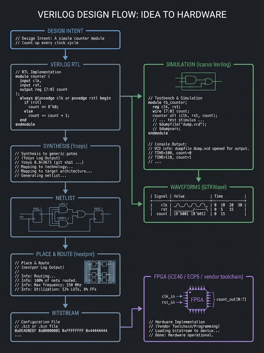
Big picture diagram (idea to hardware):
Design intent
   |
   v
Verilog RTL  -->  Simulation (Icarus Verilog)  -->  Waveforms (GTKWave)
   |
   v
Synthesis (Yosys)  -->  Netlist
   |
   v
Place & Route (nextpnr)  -->  Bitstream
   |
   v
FPGA (iCE40 / ECP5 / vendor toolchain)
Key Terms You’ll See Everywhere
- RTL: Register Transfer Level; the synthesizable subset of Verilog you write.
- DUT: Device Under Test; the module you are simulating.
- Testbench: Simulation-only module that drives and checks the DUT.
- Combinational: Logic with no memory; outputs depend only on current inputs.
- Sequential: Logic with memory; outputs depend on inputs + state.
- Timing closure: Passing all setup/hold checks at your target clock.
- CDC: Clock Domain Crossing; any signal crossing between unrelated clocks.
- Constraint: A rule (SDC/XDC) describing clocks and I/O timing to tools.
How to Use This Guide
- Read the mini-book primer first. It builds the mental model that prevents common HDL mistakes.
- Build projects in order. Each project maps to one or more theory chapters.
- Simulate everything. Waveforms are your debugger and your proof.
- Only move to FPGA after Project 6. You need sequential logic and resets under control first.
- Record evidence. Keep a lab notebook with screenshots of waveforms and timing notes.
- Use the Definition of Done for every project to verify completeness.
- Re-run tests after every change. Hardware bugs are often caused by one missing assignment.
- Treat timing like a feature. Once you move to hardware, your design must meet real setup/hold rules.
Prerequisites & Background Knowledge
Essential Prerequisites (Must Have)
Programming Skills
- Basic control flow (if/else, loops) and functions
- Comfortable with a text editor and CLI
- Able to read and edit multiple files per project
Digital Logic Fundamentals
- Boolean algebra (AND/OR/NOT/XOR) and truth tables
- Binary/hex arithmetic and bit operations
- Basic timing diagrams (edges, pulses, propagation)
- Conceptual difference between combinational vs sequential logic
Recommended reading: Digital Design and Computer Architecture, 2nd Ed – Ch. 1-3
Helpful But Not Required
- Basic electronics (voltage levels, pull-ups, input noise)
- C or Python (for tooling and testbenches)
- Computer architecture vocabulary (registers, ALU, PC)
- Familiarity with Makefiles or simple build scripts
- Linux basics (file permissions, package management)
Self-Assessment Questions
- Can you explain what a clock does in a digital system?
- Can you convert
0x3Cto binary without a calculator? - Do you know the difference between a
wireand areg? - Can you run
iverilogand view a.vcdin GTKWave? - Can you explain why a missing
elsecan create a latch? - Can you explain what setup and hold mean in one sentence each?
- Can you describe what a testbench does and why it doesn’t synthesize?
If any answer is “no”, spend 1-2 days reviewing digital logic basics first.
Development Environment Setup
Required tools (free):
- Icarus Verilog (simulation, Verilog-2005 + partial SystemVerilog support)
- GTKWave (waveform viewer for VCD/FST and more)
Recommended tools (optional but powerful):
- Verilator (linting and fast simulation for larger designs)
- OSS CAD Suite (bundled open-source FPGA tools)
- Python 3 (test generation, golden models, helpers)
Open-source FPGA flow (when you get hardware):
- Yosys (synthesis)
- nextpnr (place & route)
- Project IceStorm (iCE40 bitstream tools)
- Project Trellis (ECP5 bitstream tools)
Formal verification (optional):
- SymbiYosys (SBY) (front-end for Yosys-based formal flows)
Optional hardware (after Project 6):
- TinyFPGA BX (iCE40)
- iCEBreaker (iCE40)
- ULX3S (ECP5)
Install examples:
# macOS
brew install icarus-verilog gtkwave yosys nextpnr-ice40 icestorm

# Ubuntu/Debian
sudo apt install iverilog gtkwave
# For open-source FPGA flow, use distro packages or OSS CAD Suite.
Testing your setup:
# Verify tools are on PATH
which iverilog vvp gtkwave

# Compile a tiny design + testbench
cat > and.v <<'EOF'
module and2(input a, input b, output y);
  assign y = a & b;
endmodule
EOF

cat > and_tb.v <<'EOF'
module and_tb;
  reg a=0, b=0; wire y;
  and2 dut(.a(a), .b(b), .y(y));
  initial begin
    $dumpfile("and.vcd"); $dumpvars(0,and_tb);
    #1 a=1; #1 b=1; #1 $finish;
  end
endmodule
EOF

iverilog -o and_tb and.v and_tb.v && vvp and_tb
ls and.vcd
Time Investment
- Beginner projects: 2-4 hours each
- Intermediate projects: 4-8 hours each
- Advanced projects: 1-2 weeks each
- Final CPU: 4-8 weeks
Important Reality Check
Hardware is unforgiving. A single missing assignment can create a latch. A single timing path can break your design on real silicon. This is normal. The payoff is deep, real understanding of how computers work.
Big Picture / Mental Model
A digital system is a pipeline of combinational logic and state that advances on clock edges:
Inputs  -->  Combinational Logic  -->  Registers  -->  Combinational Logic  -->  Outputs
                   ^                         |
                   |                         v
               (always @*)            (always @(posedge clk))
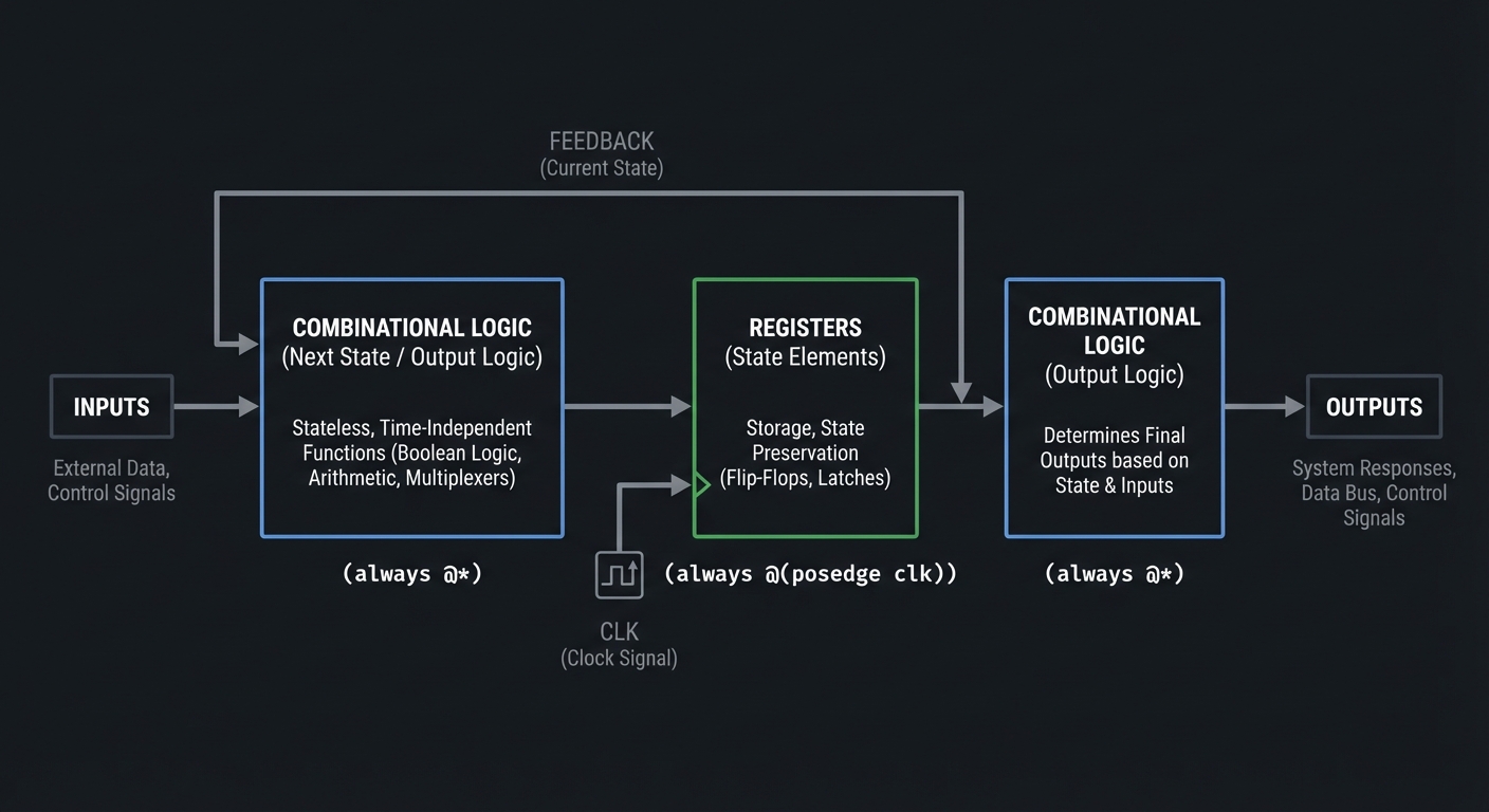
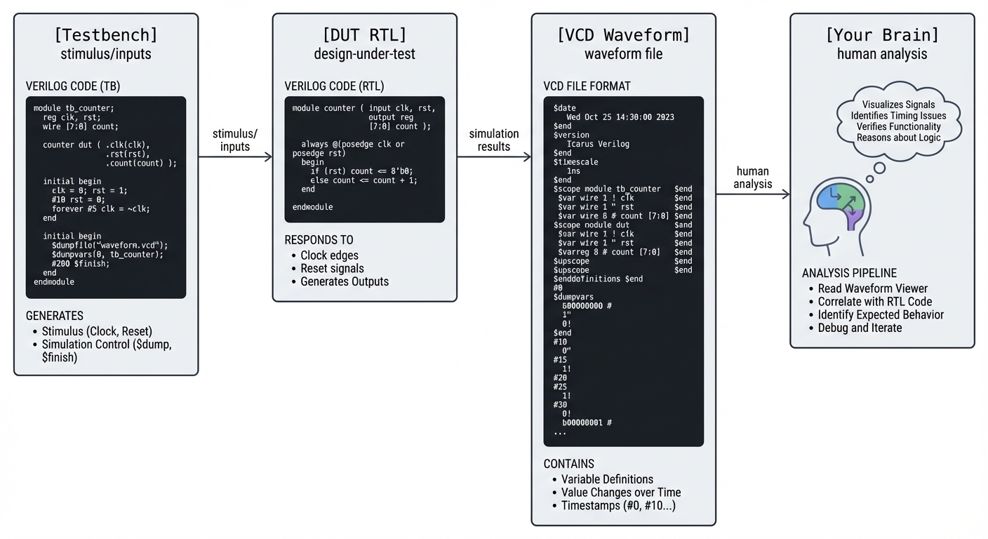
Simulation is how you see that pipeline in motion:
[Testbench] -> [DUT RTL] -> [VCD Waveform] -> [Your Brain]
Simulation scheduling (single time step):
Time t
  Active events: blocking assignments update immediately
  NBA region: non-blocking updates are queued
  End of time step: all NBA updates commit together
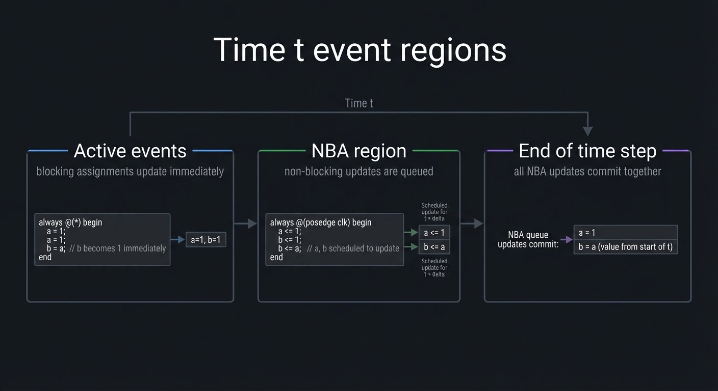
Mental model: blocking models immediate combinational behavior; non-blocking models edge-triggered state updates that all commit together.
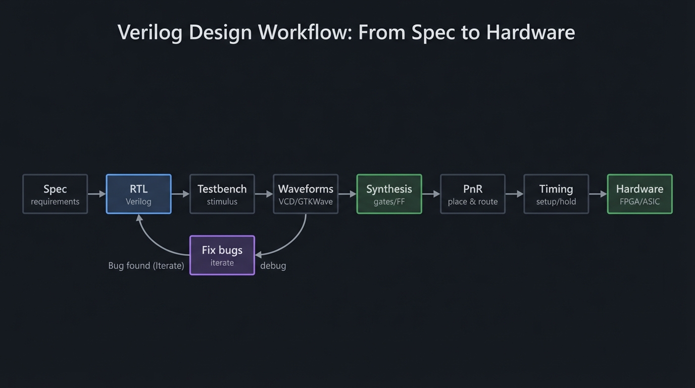
Another way to view the whole workflow:
Spec -> RTL -> Testbench -> Waveforms -> Fix bugs -> Synthesis -> PnR -> Timing -> Hardware
Clock-domain view (why synchronizers exist):
clkA domain                 clkB domain
  [logic] ---> async signal ---> [2-FF sync] ---> [logic]
Theory Primer (Mini-Book)
Chapter 1: Hardware vs Software Thinking
Definitions & Key Terms
- HDL: A language that describes hardware structure and behavior.
- Parallelism: All hardware components are active simultaneously.
- RTL: Register Transfer Level modeling of data movement and control.
Mental Model Diagram
Software:                     Hardware:
Step1 -> Step2 -> Step3       Gate A + Gate B + Gate C
                              all active at once
How It Works (Step-by-Step)
- You describe logic as structure (modules and wires).
- Simulation evaluates signal changes concurrently.
- Synthesis converts logic to gates and flip-flops.
- The FPGA implements those gates physically.
Trade-Offs
- Hardware is parallel but uses fixed resources.
- Software is flexible but sequential.
Minimal Concrete Example
assign out = a & b; // combinational gate
Common Misconceptions
- “Verilog runs top to bottom.” (No, it is concurrent.)
- “if/else is control flow.” (No, it is a hardware multiplexer.)
Check-Your-Understanding
- When does
outchange ifachanges? - What hardware does an
assignrepresent? - Why can two always blocks run at the same time?
Where You’ll Apply It
Projects 1-20 and Final CPU.
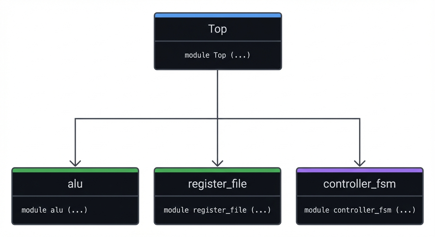
Chapter 2: Modules, Hierarchy, and Structural Design
Definitions & Key Terms
- Module: A hardware block with ports (inputs/outputs/inouts).
- Instance: A placed copy of a module.
- Hierarchy: Composition of modules into larger systems.
Mental Model Diagram
Top
|-- alu
|-- register_file
|-- controller_fsm
How It Works (Step-by-Step)
- Define small, testable modules.
- Connect them with named wires at a higher level.
- Reuse modules by instantiating them multiple times.
- Verify each module independently, then integrate.
Trade-Offs
- Deep hierarchy improves reuse but can hide timing problems.
- Flat designs are simple but harder to maintain.
Minimal Concrete Example
module top(input clk, input [7:0] a, b, output [7:0] y);
  wire [7:0] sum;
  adder8 u_add(.a(a), .b(b), .y(sum));
  reg8  u_reg(.clk(clk), .d(sum), .q(y));
endmodule
Common Misconceptions
- “Modules imply clocked logic.” (No, modules can be purely combinational.)
- “Hierarchy is only for code organization.” (It also affects timing and reuse.)
Check-Your-Understanding
- Why is a register placed after the adder in
top? - What signal is a module boundary really representing?
- When would you flatten a design?
Where You’ll Apply It
Projects 4-20 and Final CPU.
Chapter 3: Signals, Types, and 4-State Logic
Definitions & Key Terms
- wire: A net driven by continuous assignments.
- reg: A procedural variable that may infer storage.
- 4-state logic: 0, 1, X (unknown), Z (high-impedance).
- Vector: Multi-bit signal (
[7:0]).
Mental Model Diagram
wire: source ----->-----> destination
reg:  [storage] (updates on events)
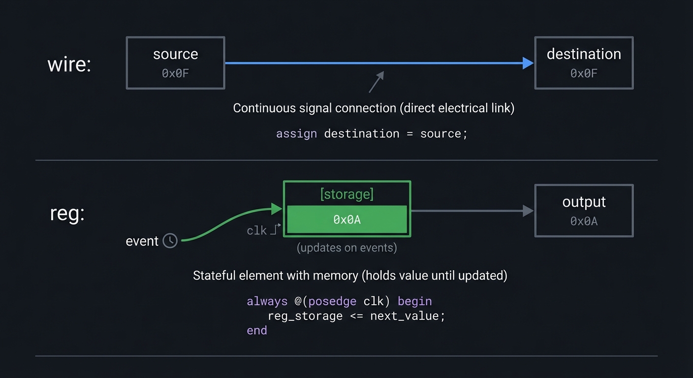
How It Works (Step-by-Step)
- Nets are driven by gates or assigns.
- Procedural variables update inside always blocks.
- Conflicting drivers cause X in simulation.
- Z represents tri-state or disconnected lines.
Trade-Offs
- 4-state logic catches bugs but only exists in simulation.
regis a simulation variable, not always a flip-flop.
Minimal Concrete Example
wire y;
reg  a;
assign y = a;
Common Misconceptions
- “reg means hardware register.” (It only means a variable.)
- “X is a hardware value.” (X is a simulation warning.)
Check-Your-Understanding
- Why does X appear in waveforms?
- When does a
reginfer storage? - What is Z used for?
Where You’ll Apply It
Projects 1-14, 18-20, Final CPU.
Chapter 4: Combinational Logic Modeling
Definitions & Key Terms
- Continuous assignment:
assignfor pure combinational logic. - Combinational always block:
always @(*)with full assignment. - Latch: Level-sensitive storage inferred by missing assignment.
Mental Model Diagram
Inputs -> logic -> outputs (no memory)
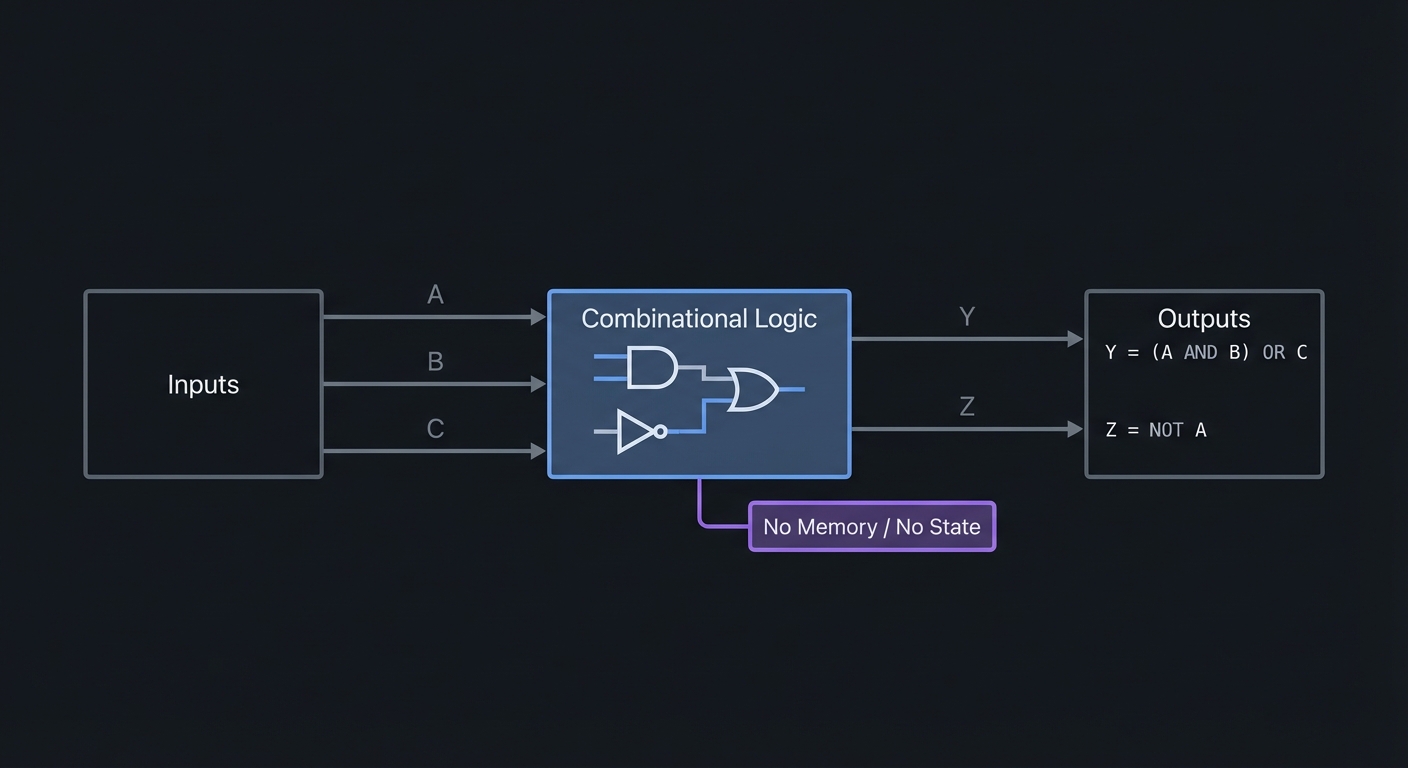
How It Works (Step-by-Step)
- Use
assignfor simple Boolean expressions. - Use
always @(*)for more complex logic or case statements. - Ensure all outputs are assigned on every path.
Trade-Offs
assignis simple but can get unwieldy.always @(*)is flexible but can create latches if incomplete.
Minimal Concrete Example
always @(*) begin
  case (sel)
    2'b00: y = a;
    2'b01: y = b;
    2'b10: y = c;
    default: y = d;
  endcase
end
Common Misconceptions
- “Missing default just means don’t care.” (It creates storage.)
- “Blocking assignments are always wrong.” (They are correct for combinational logic.)
Check-Your-Understanding
- What hardware does an if/else represent?
- Why must every path assign
y? - How do you prevent latch inference?
Where You’ll Apply It
Projects 1-5, 10, 14, 19.
Chapter 5: Sequential Logic, Clocks, and Resets
Definitions & Key Terms
- Flip-flop: Edge-triggered storage element.
- Non-blocking assignment:
<=for clocked logic. - Reset: Returns state to a known value.
- Synchronous reset: Reset sampled on clock edge.
- Asynchronous reset: Reset can change state immediately.
Mental Model Diagram
clk edge -> [FF] -> state updates
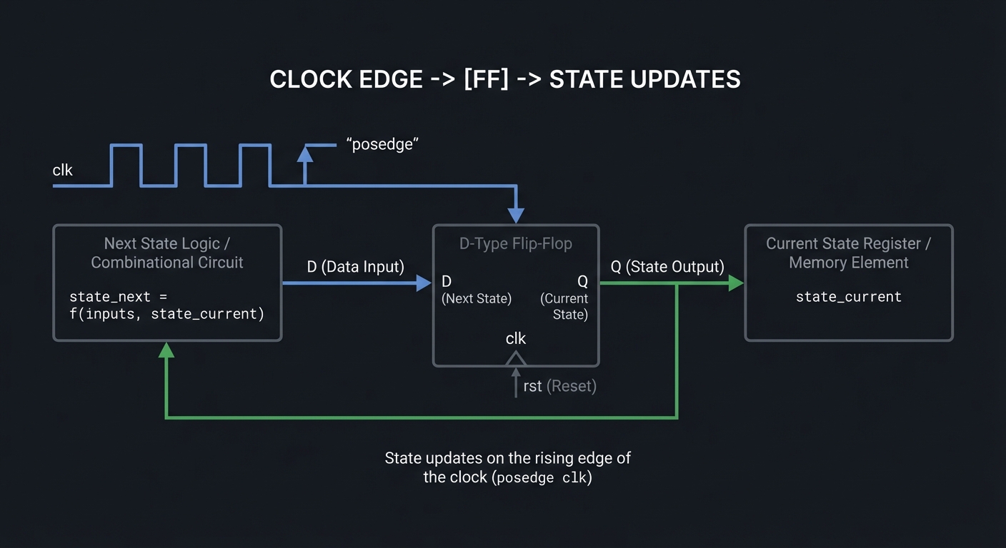
How It Works (Step-by-Step)
always @(posedge clk)models flip-flops.- Use non-blocking assignments for all state updates.
- Apply reset in the clocked block (sync) or sensitivity list (async).
Trade-Offs
- Synchronous resets are timing-friendly; asynchronous resets are immediate.
- Too much reset logic can increase area and delay.
Minimal Concrete Example
always @(posedge clk) begin
  if (reset) q <= 1'b0;
  else q <= d;
end
Common Misconceptions
- “Blocking is fine in clocked logic.” (It can create simulation mismatches.)
- “Reset always fixes bugs.” (It only gives a known starting point.)
Check-Your-Understanding
- Why use non-blocking assignments for registers?
- What can go wrong with async resets crossing domains?
- When is a reset actually needed?
Where You’ll Apply It
Projects 6-20, Final CPU.
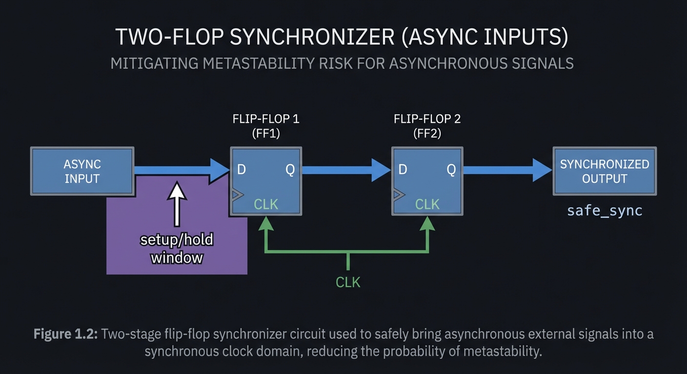
Chapter 6: Timing, Metastability, and Clock Domain Crossing
Definitions & Key Terms
- Setup/hold time: Requirements around clock edge sampling.
- Critical path: Longest delay path limiting clock speed.
- Metastability: Unstable state when sampling async inputs.
- Synchronizer: Chain of flip-flops to reduce metastability risk.
Mental Model Diagram
async_in -> FF1 -> FF2 -> safe_sync
             ^ setup/hold window
How It Works (Step-by-Step)
- Registers sample on clock edges.
- Data changing too close to the edge can go metastable.
- Long combinational paths limit maximum frequency.
- Synchronizer chains reduce but never eliminate metastability.
Trade-Offs
- Faster clocks reduce latency but risk timing failure.
- Synchronizers add latency but improve reliability.
Minimal Concrete Example
always @(posedge clk) begin
  sync1 <= async_in;
  sync2 <= sync1;
end
Common Misconceptions
- “Simulation guarantees timing correctness.” (Real delays matter.)
- “Metastability is too rare to care.” (It will show up on hardware.)
Check-Your-Understanding
- What is a critical path?
- Why use a 2-flop synchronizer?
- What does a timing constraint actually constrain?
Where You’ll Apply It
Projects 8-20, Final CPU.
Chapter 7: Finite State Machines (FSMs)
Definitions & Key Terms
- State: Encoded representation of system condition.
- Moore FSM: Outputs depend only on state.
- Mealy FSM: Outputs depend on state and inputs.
Mental Model Diagram
State A --> State B --> State C
   ^                       |
   +-----------------------+
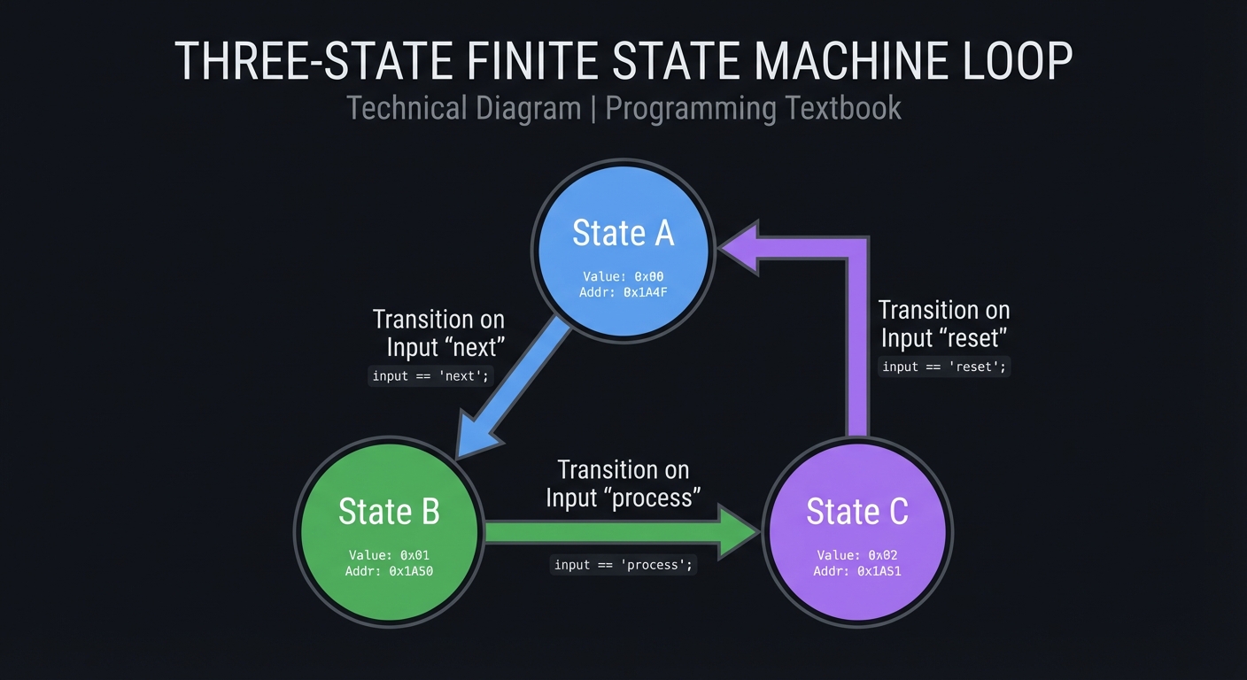
How It Works (Step-by-Step)
- Define states and transitions.
- Encode states (binary, one-hot, gray).
- Implement next-state logic and outputs.
Trade-Offs
- Moore is simpler; Mealy is faster but can glitch.
- One-hot uses more flops but simpler logic.
Minimal Concrete Example
always @(posedge clk) begin
  if (reset) state <= IDLE;
  else state <= next_state;
end

always @(*) begin
  case (state)
    IDLE: next_state = start ? RUN : IDLE;
    RUN:  next_state = done ? IDLE : RUN;
  endcase
end
Common Misconceptions
- “FSMs are only for controllers.” (UART, VGA, CPU all use FSMs.)
- “State encoding doesn’t matter.” (It affects speed and area.)
Check-Your-Understanding
- When do outputs change in Moore vs Mealy?
- Why is one-hot common in FPGAs?
- How do you avoid combinational loops in next-state logic?
Where You’ll Apply It
Projects 11-13, 15-20, Final CPU.
Chapter 8: Datapaths, Memory, and ALUs
Definitions & Key Terms
- Datapath: Data processing path (ALU + registers + muxes).
- RAM inference: Modeling memory with arrays in RTL.
- Register file: Collection of registers with read/write ports.
Mental Model Diagram
Registers -> ALU -> Registers -> Memory
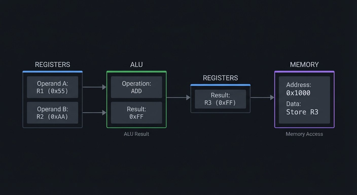
How It Works (Step-by-Step)
- Registers hold operands.
- ALU computes results based on opcode.
- Results store to registers or memory.
- Memory can be synchronous (clocked) or asynchronous.
Trade-Offs
- Wider datapaths use more resources.
- Block RAM is smaller and faster than flip-flop arrays.
Minimal Concrete Example
reg [7:0] mem [0:255];

always @(posedge clk) begin
  if (we) mem[addr] <= din;
  dout <= mem[addr];
end
Common Misconceptions
- “Memories behave like combinational arrays.” (Most are synchronous.)
- “ALU is just adders.” (It needs op selection and flags.)
Check-Your-Understanding
- What is the difference between sync and async RAM?
- Why separate datapath and control?
- What is the timing cost of a wide mux?
Where You’ll Apply It
Projects 4-7, 14, 19, Final CPU.
Chapter 9: Verification and Testbenches
Definitions & Key Terms
- Testbench: Simulation-only module that drives inputs.
- VCD: Value Change Dump waveform file.
- Timescale: Simulation time unit/precision.
Mental Model Diagram
[Testbench] -> [DUT] -> [Waveforms]
How It Works (Step-by-Step)
- Testbench sets initial values.
- Stimuli are applied over time.
- Waveforms are dumped to VCD.
- GTKWave visualizes signal transitions.
Trade-Offs
- Simple tests are quick but miss corner cases.
- Random tests find bugs but take longer.
Minimal Concrete Example
initial begin
  $dumpfile("wave.vcd");
  $dumpvars(0, tb);
  a = 0; b = 0; #10;
  a = 1; b = 0; #10;
  $finish;
end
Common Misconceptions
- “Waveforms are optional.” (They are your best debugger.)
- “If it simulates, it will synthesize.” (Not always.)
Check-Your-Understanding
- Why separate testbench from DUT?
- What does
$dumpvarsdo? - How do you make testbenches deterministic?
Where You’ll Apply It
Every project.
Chapter 10: Synthesis, Constraints, and FPGA Architecture
Definitions & Key Terms
- Synthesis: HDL to gates and flip-flops.
- Constraints: Timing and I/O rules for the implementation tools.
- LUT: Lookup table that implements logic in FPGAs.
- BRAM/DSP: Dedicated memory and arithmetic blocks.
Mental Model Diagram
RTL -> Synth -> Netlist -> PnR -> Bitstream -> FPGA fabric (LUT/FF/BRAM/DSP)
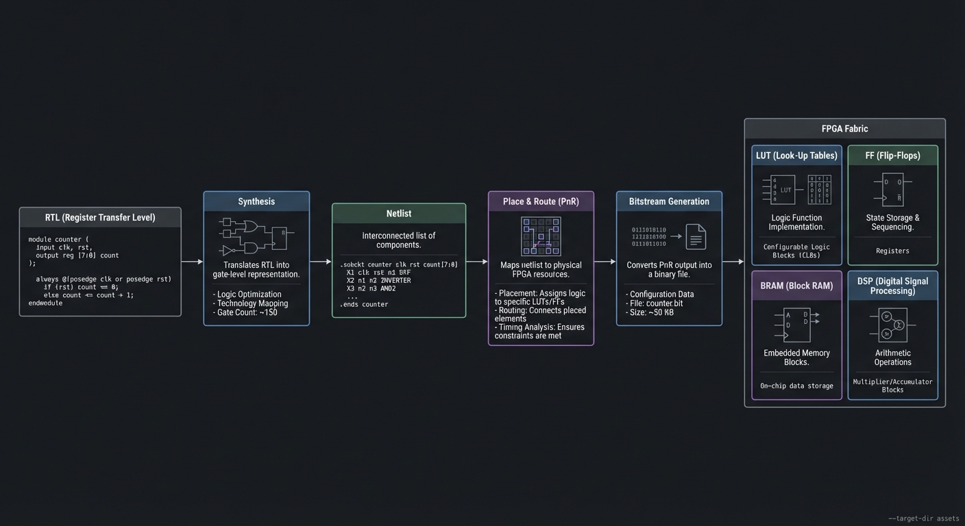
How It Works (Step-by-Step)
- Synthesis creates a netlist of logic.
- Place-and-route maps logic to FPGA resources.
- Timing analysis checks constraints.
- Bitstream configures the FPGA at power-up.
Trade-Offs
- Aggressive timing constraints can fail to close.
- Using BRAM/DSP blocks improves performance but limits flexibility.
Minimal Concrete Example
# iCE40 open-source flow
yosys -p "synth_ice40 -json top.json" top.v
nextpnr-ice40 --hx8k --json top.json --asc top.asc
icepack top.asc top.bin
iceprog top.bin
Common Misconceptions
- “The FPGA runs at any clock I want.” (Timing closure is real.)
- “Synthesis errors are like compiler errors.” (They are hardware limits.)
Check-Your-Understanding
- What does synthesis produce?
- Why are constraints required?
- What FPGA resources are best for multipliers?
Where You’ll Apply It
Projects 8-20, Final CPU.
Chapter 11: Interfaces and Peripherals
Definitions & Key Terms
- UART: Asynchronous serial protocol with 1 start bit (low), 5-9 data bits (LSB-first), optional parity, and 1-2 stop bits (high); line idles high.
- SPI: Synchronous serial protocol with CPOL/CPHA modes (0-3) that define sample/shift edges.
- PWM: Duty-cycle based control for brightness/servo.
- VGA: Video output using sync pulses and pixel stream.
Mental Model Diagram
UART: idle(1) start(0) data bits LSB-first stop(1)
SPI:  SCK + MOSI + MISO + CS, sample on edges
VGA:  HSYNC/VSYNC + RGB pixel stream
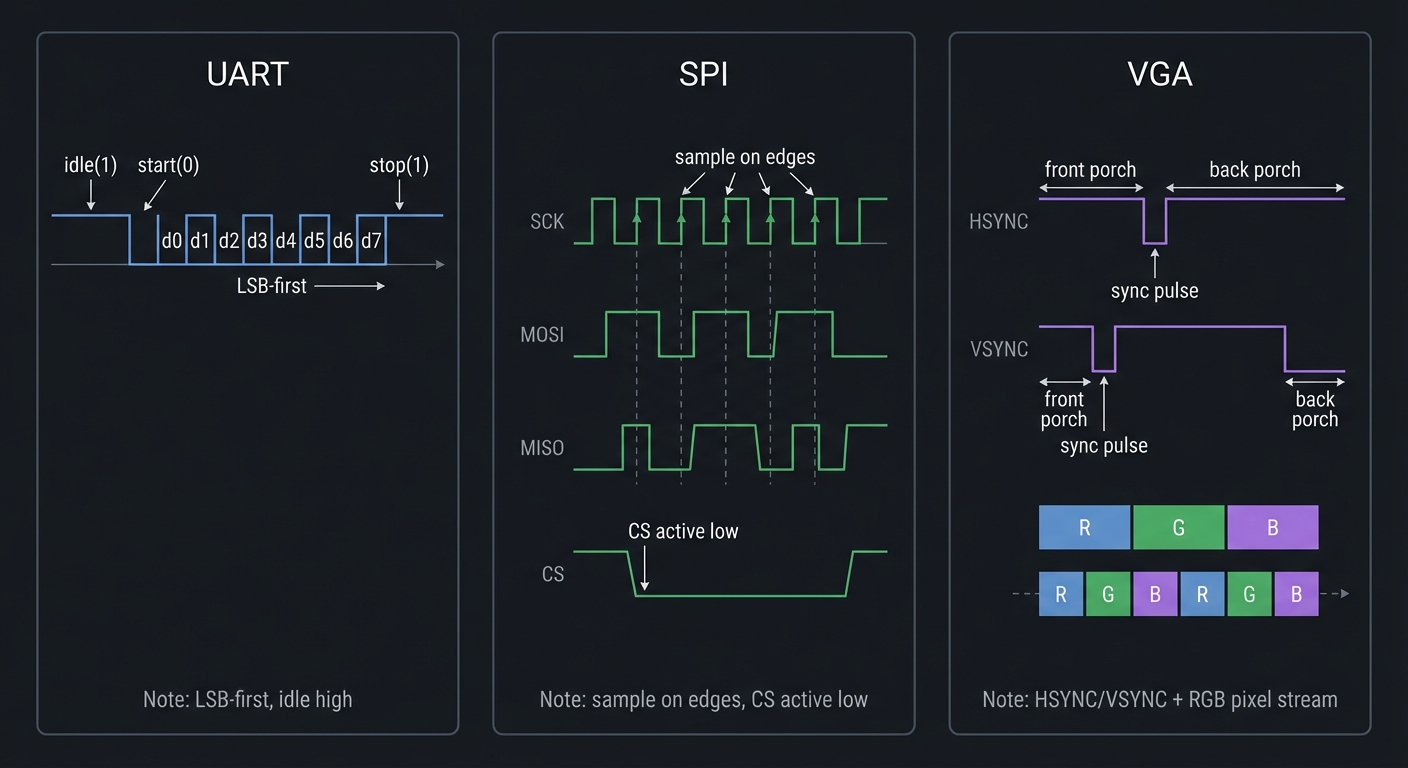
How It Works (Step-by-Step)
- UART frames bytes with 1 start bit, 5-9 data bits, optional parity, and 1-2 stop bits; data is LSB-first and idle is high.
- SPI uses a shared clock; CPOL/CPHA select sampling and shifting edges across four modes.
- PWM controls average voltage using duty cycle.
- VGA streams pixels at fixed timing with porches and sync.
SPI mode quick reference:
- Mode 0: CPOL=0, CPHA=0 (sample on rising edge)
- Mode 1: CPOL=0, CPHA=1 (sample on falling edge)
- Mode 2: CPOL=1, CPHA=0 (sample on falling edge)
- Mode 3: CPOL=1, CPHA=1 (sample on rising edge)
UART 8N1 = 8 data bits, No parity, 1 stop bit.
Trade-Offs
- UART is simple but slower and less robust than clocked protocols.
- SPI is fast but uses more wires and requires exact mode matching.
- VGA timing is strict and unforgiving.
Minimal Concrete Example
// UART TX: shift register driven by baud tick
if (baud_tick) begin
  tx <= shift[0];
  shift <= {1'b1, shift[9:1]};
end
Common Misconceptions
- “UART is clocked.” (It is asynchronous.)
- “SPI modes don’t matter.” (They must match the slave.)
- “VGA timing is flexible.” (It is rigid.)
Check-Your-Understanding
- What does 8N1 mean?
- What do CPOL and CPHA control?
- Why does VGA need blanking intervals?
Where You’ll Apply It
Projects 10, 15-20.
Chapter 12: Debugging and Hardware Bring-Up
Definitions & Key Terms
- Bring-up: First time a design runs on hardware.
- Logic analyzer: Tool to capture internal or external signals.
- In-system debugging: Probing internal signals on FPGA.
Mental Model Diagram
Bug -> waveform -> hypothesis -> fix -> re-simulate -> reprogram
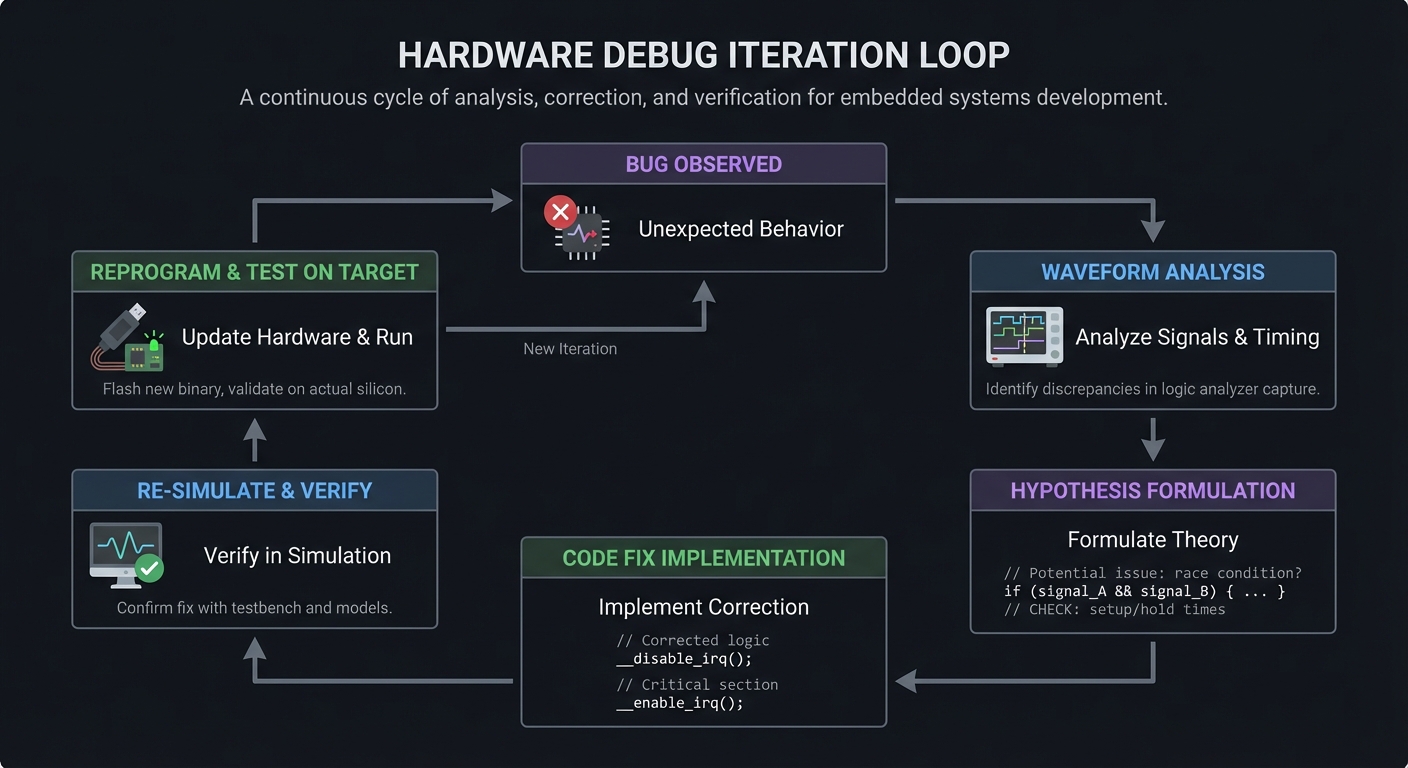
How It Works (Step-by-Step)
- Reproduce the bug in simulation first.
- Add probes and capture waveforms.
- Compare expected vs actual transitions.
- Fix logic and re-verify.
Trade-Offs
- Extra probes increase resource usage.
- On-hardware debugging is slower but sometimes necessary.
Minimal Concrete Example
// Example debug probe
reg [7:0] dbg_state;
always @(posedge clk) dbg_state <= state;
Common Misconceptions
- “Hardware debug is just like software debugging.” (It’s not.)
- “If it works once, it’s fine.” (Timing bugs can be intermittent.)
Check-Your-Understanding
- Why should you debug in simulation first?
- What is the cost of adding debug probes?
- How do you validate a fix?
Where You’ll Apply It
Projects 8-20, Final CPU.
Chapter 13: Simulation Semantics and Event Scheduling
Definitions & Key Terms
- Delta cycle: A zero-time simulation step used to settle combinational logic.
- Event queue: The simulator’s ordered list of events to process.
- Active region: Where blocking assignments update immediately.
- NBA region: Where non-blocking assignments update at the end of the time step.
Mental Model Diagram
Time t:
  Active (blocking)  ->  Inactive  ->  NBA (non-blocking)  ->  Time t+1
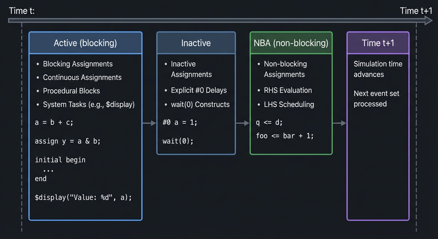
How It Works (Step-by-Step)
- Inputs change, scheduling events in the active region.
- Blocking assignments update immediately and can trigger more active events.
- Non-blocking assignments schedule updates for the NBA region.
- At the end of the time step, NBA updates commit simultaneously.
Trade-Offs
- Blocking is intuitive for combinational logic but dangerous for sequential state.
- Non-blocking avoids race conditions but requires a clear mental model.
Minimal Concrete Example
// Two always blocks racing if you use blocking
always @(posedge clk) a = b;
always @(posedge clk) b = a; // race if blocking, safe if non-blocking
Common Misconceptions
- “Blocking and non-blocking are interchangeable.” (They are not.)
- “Simulation order equals hardware order.” (Hardware is concurrent.)
Check-Your-Understanding
- What happens if two always blocks assign the same reg in the same time step?
- Why do non-blocking assignments reduce race conditions?
- What is a delta cycle and why does it exist?
Where You’ll Apply It
Projects 1-20 and Final CPU (especially Projects 6-7 and all FSMs).
Chapter 14: Synthesizable Subset and Coding Patterns
Definitions & Key Terms
- Synthesizable: Can be converted into real hardware by tools.
- Latch inference: Unintended storage created by incomplete assignments.
- Combinational always block:
always @(*)with full assignment.
Mental Model Diagram
Allowed RTL -> Synthesis -> Gates/FFs
Sim-only RTL (delays, force/release) -> Simulation only
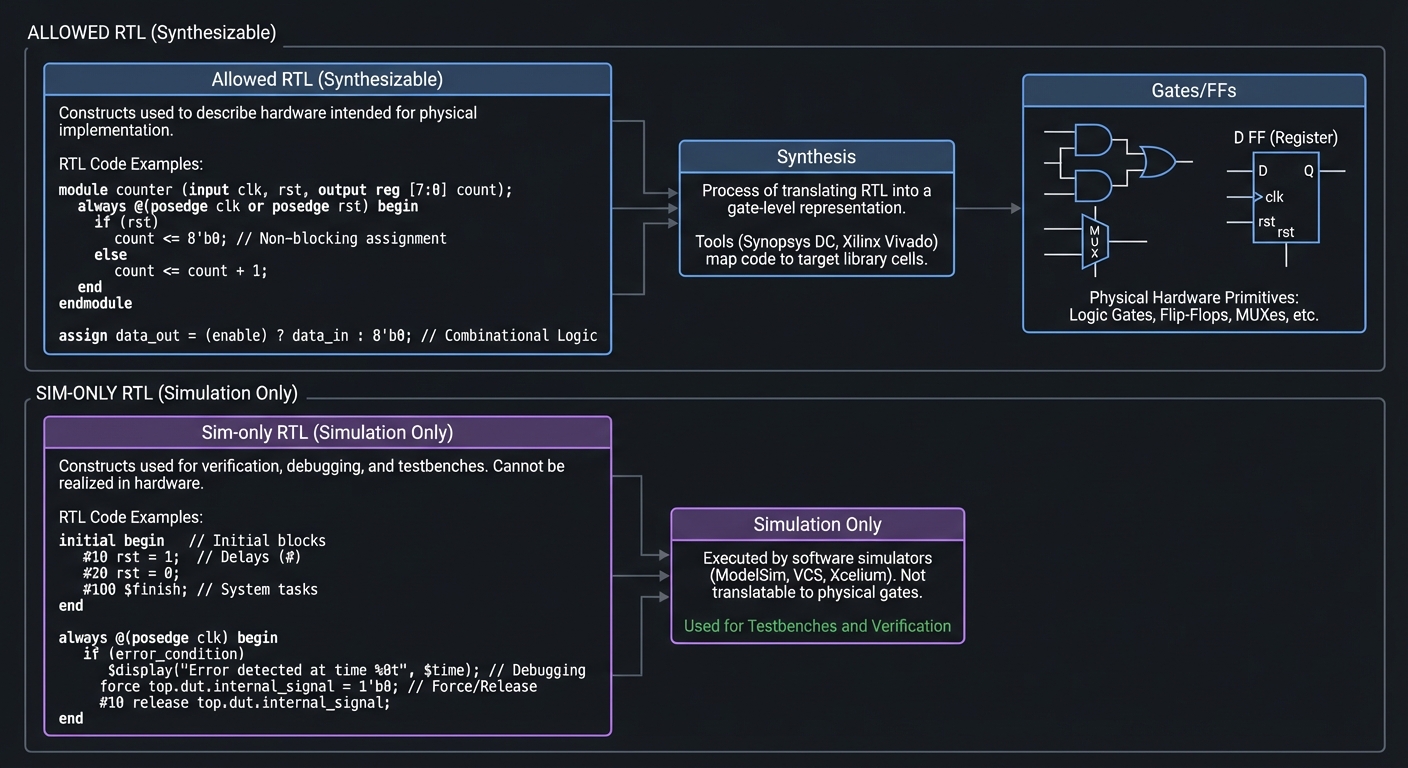
How It Works (Step-by-Step)
- Use
assignoralways @(*)for combinational logic. - Use
always @(posedge clk)for sequential logic. - Avoid
#delayandinitialfor synthesizable logic (ok in testbenches). - Give every combinational output a value on all paths.
Trade-Offs
- Strict synthesizable style reduces surprises but can feel restrictive.
- Some constructs simulate fine but will not synthesize.
Minimal Concrete Example
always @(*) begin
  y = 0;            // default prevents latch
  if (en) y = a;
end
Common Misconceptions
- “for loops mean hardware iterates.” (Loops are unrolled at compile time.)
- “initial blocks never synthesize.” (Some FPGAs allow RAM init, but not portable.)
Check-Your-Understanding
- Why does a missing
elseinfer a latch? - Which constructs are safe in testbenches but unsafe in RTL?
- When does a
forloop become hardware?
Where You’ll Apply It
Projects 1-20 and Final CPU.
Chapter 15: Reset Strategies, Clock Enables, and Safe Clocking
Definitions & Key Terms
- Clock enable: Allows a register to update only when enabled.
- Clock gating: Turning off a clock (usually not safe in FPGA without special cells).
- Reset synchronizer: Syncs an async reset into a clock domain.
Mental Model Diagram
clk ---> [FF] ---> q
         ^  ^
        rst en
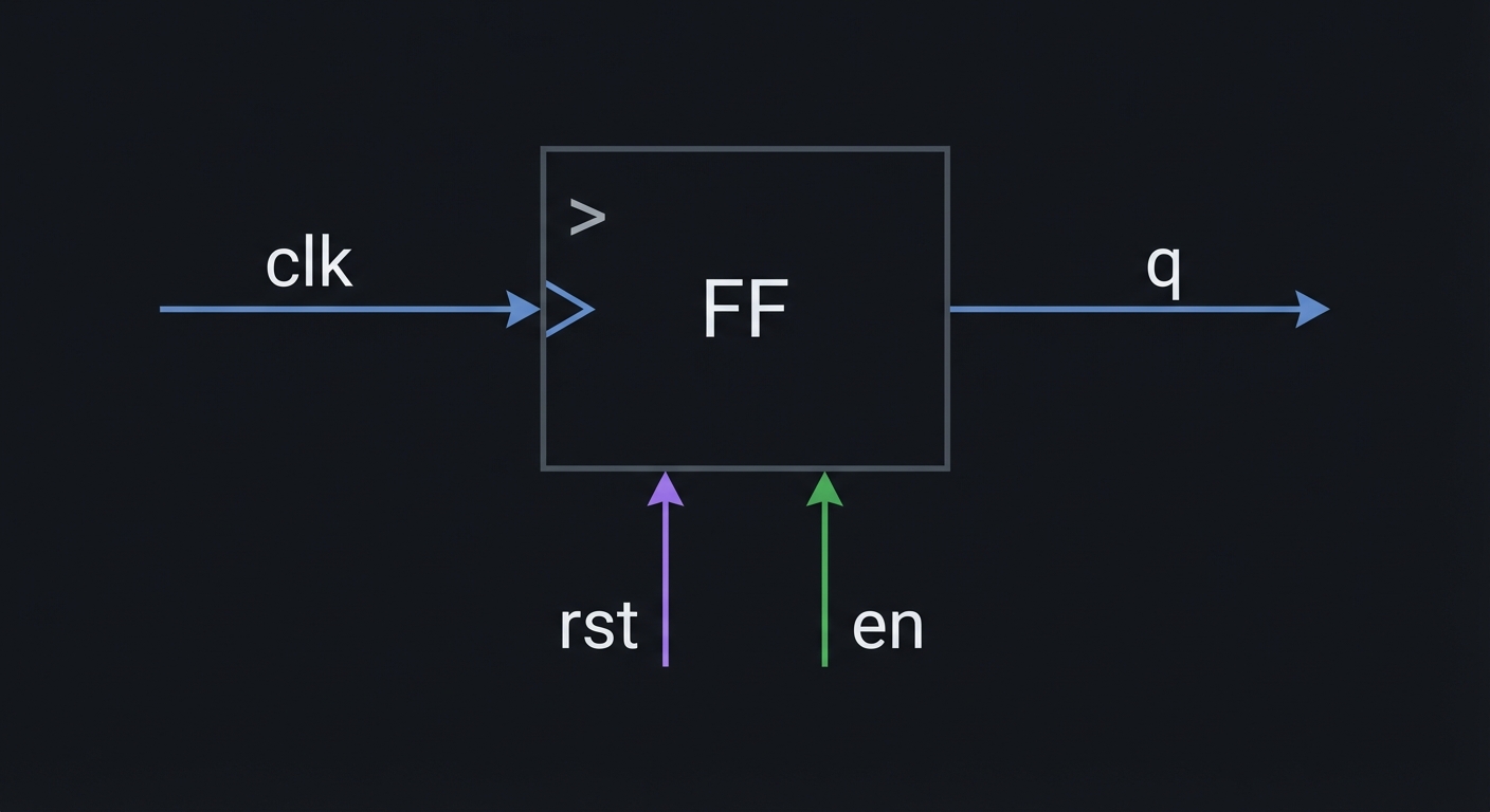
How It Works (Step-by-Step)
- Decide if reset is synchronous or asynchronous.
- If async, synchronize reset deassertion to avoid metastability.
- Use clock enables instead of gating clocks when possible.
- Document reset behavior in testbenches.
Trade-Offs
- Synchronous reset is timing-friendly but requires clock to recover.
- Asynchronous reset reacts instantly but risks CDC issues on release.
Minimal Concrete Example
always @(posedge clk) begin
  if (reset) q <= 0;
  else if (en) q <= d;
end
Common Misconceptions
- “Clock gating saves power everywhere.” (In FPGAs, use enables instead.)
- “Reset fixes timing bugs.” (It only sets initial state.)
Check-Your-Understanding
- Why is reset deassertion often synchronized?
- What is the difference between clock enable and clock gating?
- When is a reset actually necessary?
Where You’ll Apply It
Projects 6-20 and Final CPU.
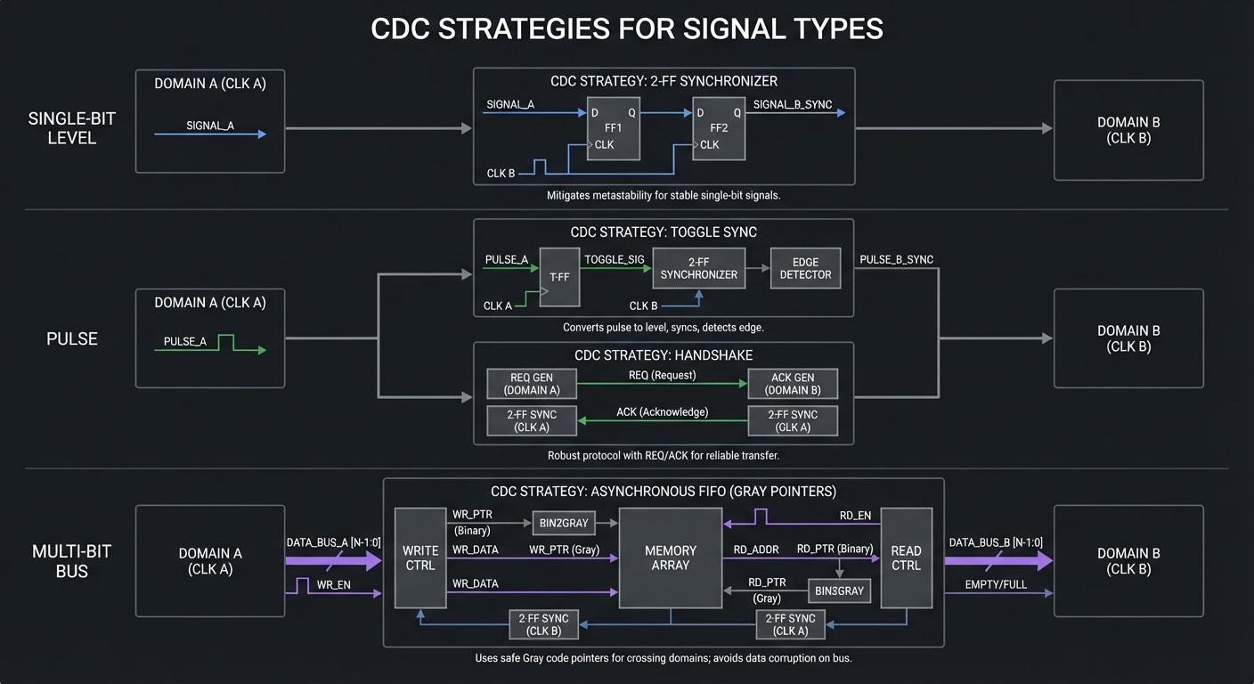
Chapter 16: CDC Design Patterns (Beyond 2-FF)
Definitions & Key Terms
- CDC: Clock domain crossing.
- Toggle synchronizer: Safely transfers pulses across clocks.
- Async FIFO: Buffers data between unrelated clocks.
- Gray code: Encoding where only one bit changes at a time.
Mental Model Diagram
clkA domain      clkB domain
   [data] --toggle--> [sync] --> [pulse]
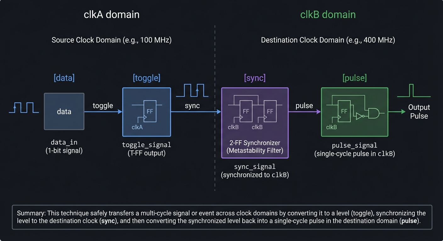
How It Works (Step-by-Step)
- Identify signals that cross clock boundaries.
- Use 2-FF synchronizers for single-bit levels.
- Use toggle or handshake for pulses.
- Use async FIFOs for multi-bit data streams.
Trade-Offs
- Simple synchronizers are cheap but add latency.
- Async FIFOs are robust but more complex to verify.
Minimal Concrete Example
// Toggle sync for a pulse
always @(posedge clkA) if (event) toggle <= ~toggle;
always @(posedge clkB) {sync1,sync2} <= {sync2,toggle};
assign pulse_b = sync1 ^ sync2;
Common Misconceptions
- “A bus can be synchronized with 2 flops.” (Only safe for 1-bit signals.)
- “Metastability can be eliminated.” (It can only be reduced.)
Check-Your-Understanding
- When should you use an async FIFO vs a synchronizer?
- Why is Gray code used in async FIFOs?
- Why do pulses need special handling across clocks?
Where You’ll Apply It
Projects 9, 15-17, 20, and Final CPU (button inputs, async serial, IO).
Chapter 17: Constraints and Static Timing Analysis
Definitions & Key Terms
- SDC/XDC: Constraint languages for clocks and I/O timing.
- STA: Static timing analysis for setup/hold verification.
- False path: A path that should not be timed.
- Multicycle path: A path that is allowed multiple cycles.
Mental Model Diagram
[FF] ---- combinational ---- [FF]
   setup/hold checked against constraints
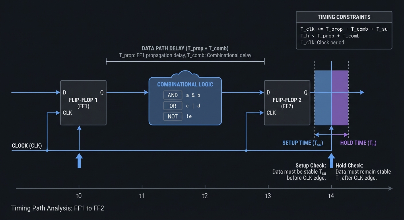
How It Works (Step-by-Step)
- Define your primary clocks.
- Constrain input/output delays relative to those clocks.
- Run STA and inspect critical paths.
- Fix timing by pipelining or reducing logic depth.
Trade-Offs
- Over-constraining can make timing closure impossible.
- Under-constraining hides real hardware failures.
Minimal Concrete Example
create_clock -name clk -period 20 [get_ports clk]
set_input_delay 2 -clock clk [get_ports rx]
set_output_delay 2 -clock clk [get_ports tx]
Common Misconceptions
- “Passing synthesis means timing is fine.” (STA is separate.)
- “Faster clock always better.” (You may fail timing.)
Check-Your-Understanding
- What is the critical path in your design?
- Why do you need input/output delays?
- When should you use a multicycle constraint?
Where You’ll Apply It
Projects 8-20 and Final CPU (hardware bring-up).
Chapter 18: FPGA Architecture and Resource Inference
Definitions & Key Terms
- LUT: Lookup table implementing combinational logic.
- Carry chain: Fast adder hardware.
- BRAM: Block RAM embedded in FPGA fabric.
- DSP slice: Dedicated multiplier/accumulator block.
Mental Model Diagram
[IO]--[LUT+FF]--[Carry]--[BRAM]--[DSP]--[IO]
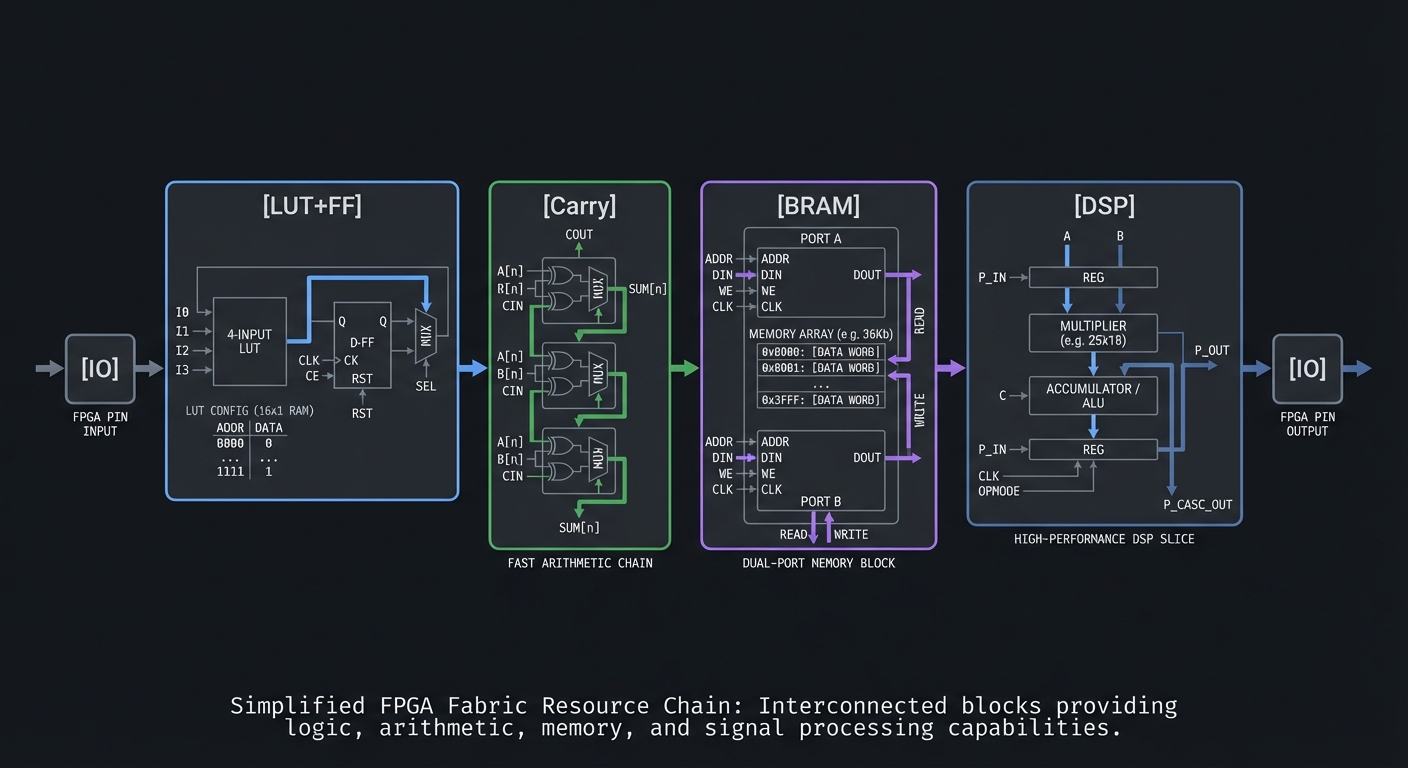
How It Works (Step-by-Step)
- Combinational logic maps to LUTs.
- Registers map to flip-flops near LUTs.
- Adders use carry chains for speed.
- Memories infer BRAM when coded appropriately.
Trade-Offs
- BRAM is fast and dense but has fixed widths.
- DSP slices are efficient but require specific coding patterns.
Minimal Concrete Example
reg [7:0] mem [0:255];
// Inference of simple RAM
always @(posedge clk) if (we) mem[addr] <= din;
Common Misconceptions
- “All logic uses LUTs equally.” (Carry chains and DSPs are special.)
- “Small RAMs always become BRAM.” (Size and coding style matter.)
Check-Your-Understanding
- Why are carry chains faster than LUT adders?
- When does memory infer BRAM vs registers?
- What coding patterns map to DSPs?
Where You’ll Apply It
Projects 4-5, 14, 18-20, Final CPU.
Chapter 19: Verification Beyond Basics
Definitions & Key Terms
- Self-checking testbench: Testbench that asserts pass/fail automatically.
- Assertion: A condition that must always be true.
- Scoreboard: Compares DUT outputs to a golden model.
Mental Model Diagram
Stimulus -> DUT -> Outputs -> Scoreboard -> PASS/FAIL
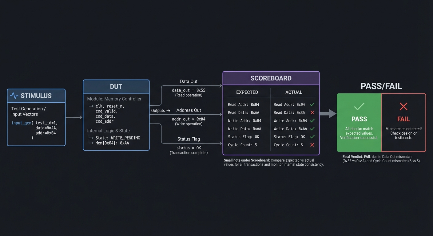
How It Works (Step-by-Step)
- Define expected behavior (golden model or reference).
- Drive stimuli and record outputs.
- Compare outputs to expected values every cycle.
- Fail fast with clear diagnostics.
Trade-Offs
- Assertions add clarity but require careful specification.
- Golden models take time but catch subtle bugs early.
Minimal Concrete Example
if (y !== expected) begin
  $display("FAIL: y=%h exp=%h", y, expected);
  $finish;
end
Common Misconceptions
- “Waveforms are enough.” (Self-checking tests scale better.)
- “Assertions are only for SystemVerilog.” (You can do checks in Verilog.)
Check-Your-Understanding
- What makes a testbench deterministic?
- Why is a scoreboard useful for complex designs?
- How would you add a random test while keeping reproducibility?
Where You’ll Apply It
All projects, especially Projects 5, 12, 15-20, and Final CPU.
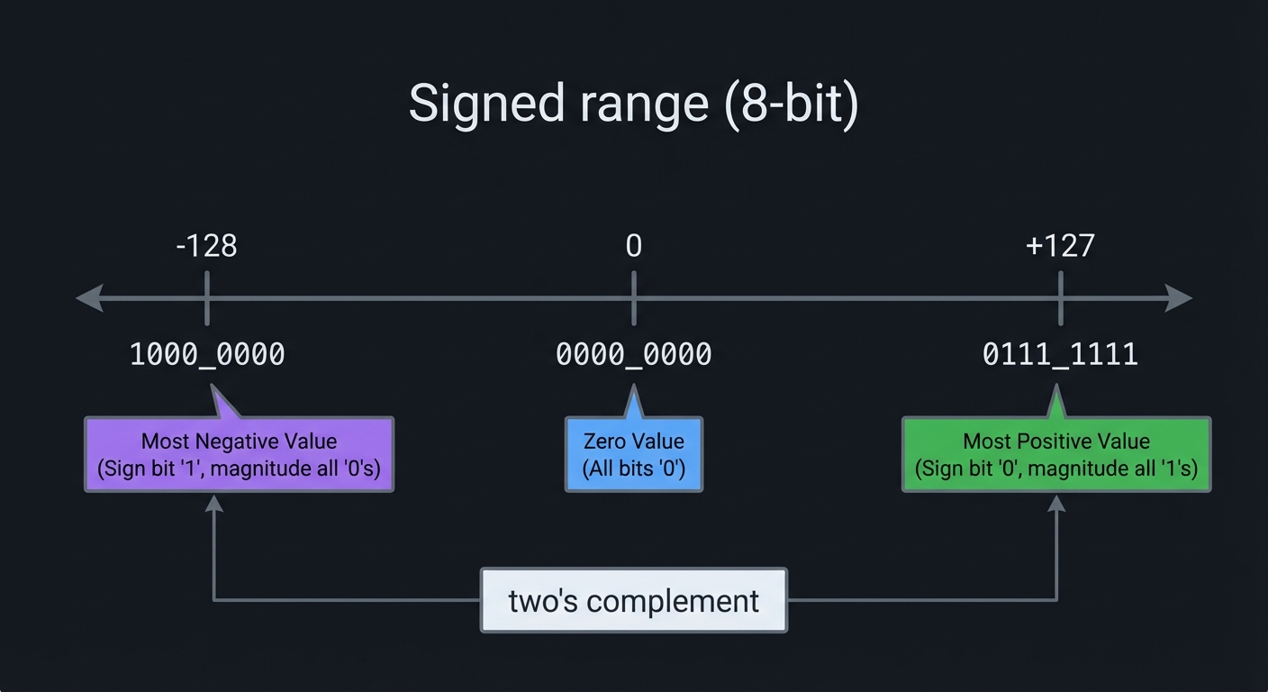
Chapter 20: Signed Arithmetic, Overflow, and Fixed-Point
Definitions & Key Terms
- Signed: Two’s complement numbers with a sign bit.
- Unsigned: Numbers without sign; all bits are magnitude.
- Sign extension: Replicating sign bit when widening signed values.
- Overflow: Result doesn’t fit the signed range (carry != overflow).
- Fixed-point: Integer representation of fractional values (Qm.n format).
Mental Model Diagram
Signed range (8-bit):
-128 --------------------- 0 --------------------- +127
 1000_0000                0000_0000                0111_1111
How It Works (Step-by-Step)
- Decide whether signals are
signedorunsignedup front. - When widening, sign-extend signed values (
{ {N{a[MSB]}}, a }). - Detect signed overflow by comparing operand sign bits to result sign bit.
- For fixed-point multiply, multiply full width then drop fractional bits.
Trade-Offs
- Signed math is more expressive but can hide overflow unless you check.
- Fixed-point gives fractional precision without a floating unit, but you must manage scaling.
Minimal Concrete Example
wire signed [7:0] a, b;
wire signed [8:0] sum = a + b;  // widen to detect overflow
wire overflow = (a[7] == b[7]) && (sum[7] != a[7]);

// Fixed-point Q8.8 multiply
wire signed [15:0] prod = a * b;   // Q8.8 * Q8.8 = Q16.16
wire signed [7:0]  y    = prod[15:8]; // back to Q8.8
Common Misconceptions
- “Carry-out means signed overflow.” (Not true; overflow depends on sign bits.)
- “Unsigned literals are always safe.” (Unsized numbers are 32-bit signed by default.)
Check-Your-Understanding
- How do you detect signed overflow for addition?
- What happens if you add two negative numbers and get a positive result?
- What is the scaling step after a fixed-point multiply?
Where You’ll Apply It
Projects 4-5, 19, Final CPU.
Chapter 21: Parameterization, Generate, and Reuse
Definitions & Key Terms
- parameter: Compile-time constant that customizes a module.
- localparam: Derived constant computed from parameters.
- generate: Verilog construct to replicate hardware.
- genvar: Generate-loop index.
Mental Model Diagram
N-bit block
  [module #(WIDTH=N)]
     |-> hardware scaled at compile time
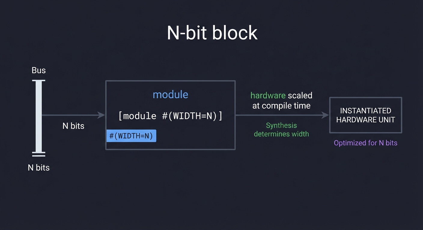
How It Works (Step-by-Step)
- Add a
parameter WIDTH = 8to your module. - Use
localparamfor derived sizes (e.g., counter width). - Use
generate+forto replicate structures. - Instantiate arrays of modules for scalable designs.
Trade-Offs
- Parameterization increases reuse but can complicate debugging.
- Generate loops are powerful but can hide accidental size mismatches.
Minimal Concrete Example
module reg_n #(parameter W=8) (
  input clk, input [W-1:0] d, output reg [W-1:0] q
);
  always @(posedge clk) q <= d;
endmodule

genvar i;
generate
  for (i=0; i<4; i=i+1) begin : GEN
    reg_n #(.W(8)) u_reg(.clk(clk), .d(bus[i]), .q(out[i]));
  end
endgenerate
Common Misconceptions
- “Parameters are runtime variables.” (They are compile-time constants.)
- “Generate loops execute in simulation.” (They unroll into hardware.)
Check-Your-Understanding
- When does a parameter value get fixed?
- What is the difference between
parameterandlocalparam? - How do you create a scalable N-bit counter?
Where You’ll Apply It
Projects 2-5, 7-8, 14, 18, Final CPU.
Chapter 22: Pipelining, Throughput, and Latency
Definitions & Key Terms
- Pipeline stage: Registers that split a long combinational path.
- Latency: Number of cycles from input to output.
- Throughput: Outputs per cycle once the pipeline is full.
- Initiation interval (II): Cycles between new inputs.
Mental Model Diagram
in -> [logic] -> (reg) -> [logic] -> (reg) -> out
          stage 1             stage 2
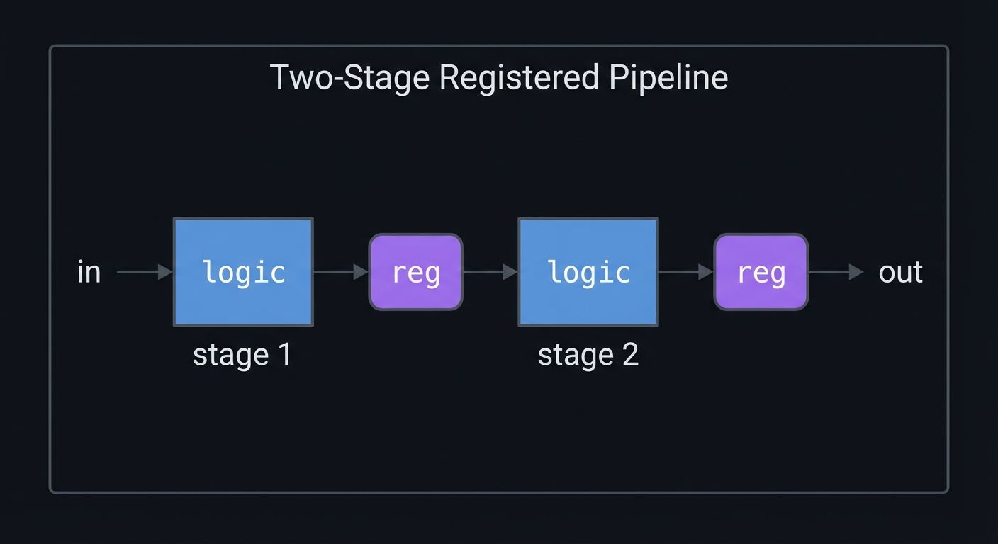
How It Works (Step-by-Step)
- Identify your critical path (longest combinational delay).
- Insert registers to split the path into stages.
- Track extra latency and update testbenches.
- Add valid signals so outputs stay aligned.
Trade-Offs
- Higher max clock speed but increased latency and register count.
- More control logic to keep data aligned across stages.
Minimal Concrete Example
always @(posedge clk) begin
  sum_stage1 <= a + b;
  sum_out    <= sum_stage1 + c;
end
Common Misconceptions
- “Pipelining always makes it faster.” (It can increase latency and complexity.)
- “Latency doesn’t matter.” (It matters for control loops and protocols.)
Check-Your-Understanding
- What is the difference between throughput and latency?
- How would you pipeline a large adder tree?
- Why do you need a valid signal in pipelines?
Where You’ll Apply It
Projects 18, 20, Final CPU (optional optimization).
Chapter 23: Handshakes, Backpressure, and Streaming Interfaces
Definitions & Key Terms
- ready/valid: Transfer occurs when both are high.
- Backpressure: Receiver throttles sender to avoid overflow.
- Skid buffer: Small buffer to decouple combinational ready paths.
- FIFO: Queue for buffering bursts and clock differences.
Mental Model Diagram
producer -> data/valid ----> consumer
             ^              |
             |---- ready <---|
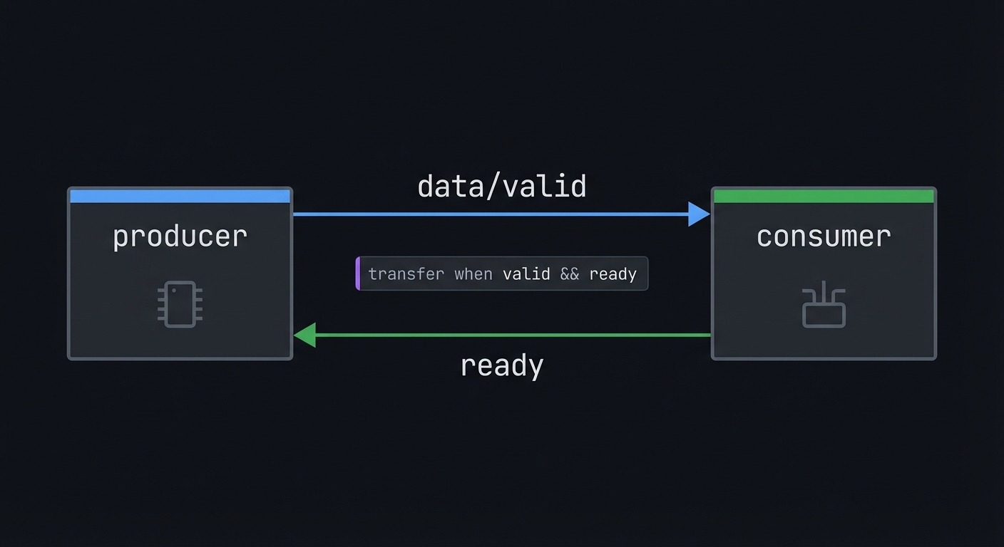
How It Works (Step-by-Step)
- Producer raises
validwhen data is stable. - Consumer raises
readywhen it can accept data. - Transfer occurs only when ready & valid are both 1.
- If consumer is slow, it deasserts
ready(backpressure).
Trade-Offs
- Extra signals and logic, but robust against stalls and bursts.
- Makes integration across modules dramatically easier.
Minimal Concrete Example
wire fire = valid & ready;
always @(posedge clk) if (fire) out <= in;
Common Misconceptions
- “valid is always a one-cycle pulse.” (It can be held high until accepted.)
- “ready must be registered.” (It can be combinational or registered, but be consistent.)
Check-Your-Understanding
- What happens if valid=1 and ready=0?
- How do you keep data stable while valid is high?
- When would you add a skid buffer?
Where You’ll Apply It
Projects 12, 15-17, Final CPU (I/O + memory interfaces).
Chapter 24: Formal Verification & Assertions (SymbiYosys)
Definitions & Key Terms
- Assertion: A property that must always hold.
- Assumption: A constraint on inputs for formal proofs.
- Cover: A property that should be reachable.
- BMC: Bounded Model Checking (searches state space to a depth).
Mental Model Diagram
RTL + Properties -> Formal engine -> PASS or counterexample waveform
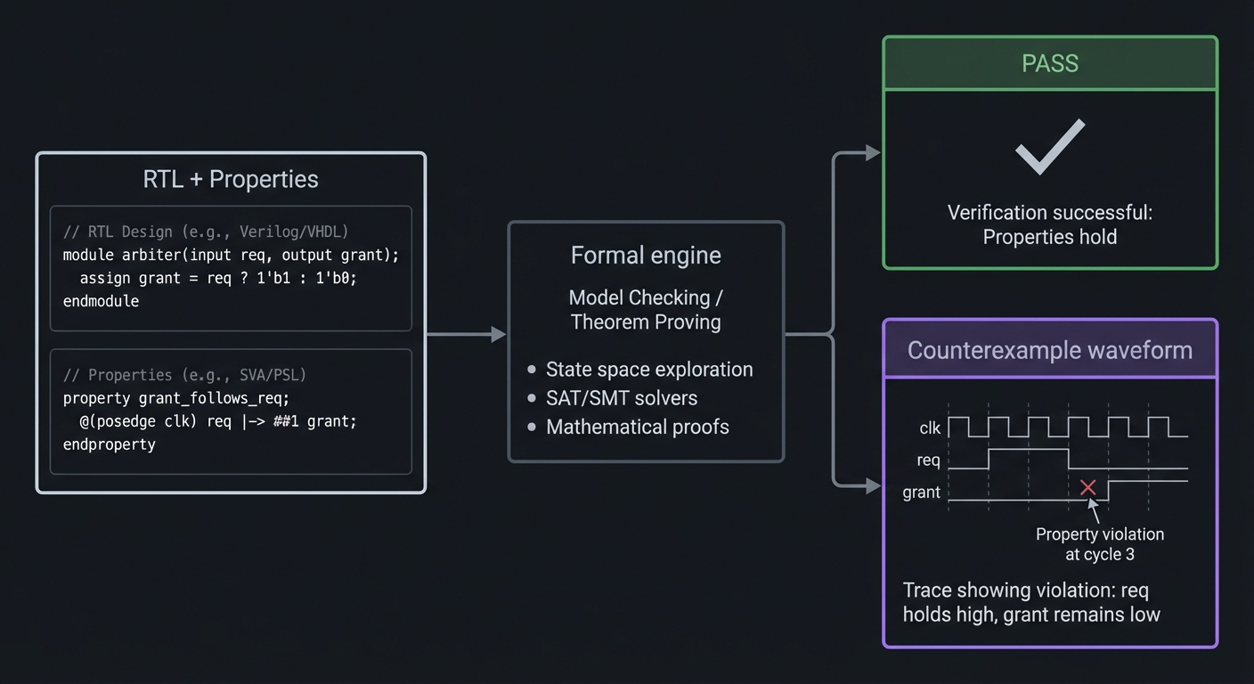
How It Works (Step-by-Step)
- Write assertions that encode your design’s intent.
- Add assumptions to constrain unrealistic inputs.
- Run SymbiYosys to search for counterexamples.
- Inspect counterexample waveforms to fix bugs.
Trade-Offs
- Finds corner-case bugs early, but only as good as your properties.
- Can be expensive on large designs without good constraints.
Minimal Concrete Example
// Counter must never skip values
always @(posedge clk) if (!reset) assert(count_next == count + 1);
Common Misconceptions
- “Formal replaces simulation.” (It complements simulation.)
- “If it passes formal, it’s perfect.” (Only properties you wrote are proven.)
Check-Your-Understanding
- What’s the difference between assert and assume?
- Why do you need to bound the search depth?
- How can a bad assumption hide a real bug?
Where You’ll Apply It
Projects 6-7, 11-13, Final CPU (optional).
Chapter 25: Linting, Coding Style, and Review Discipline
Definitions & Key Terms
- Linting: Static checks for common HDL mistakes.
- Implicit net: Undeclared wire created by a typo.
- One-driver rule: A net should have a single driver in synthesizable RTL.
Mental Model Diagram
Write RTL -> Lint -> Simulate -> Synthesize -> Hardware
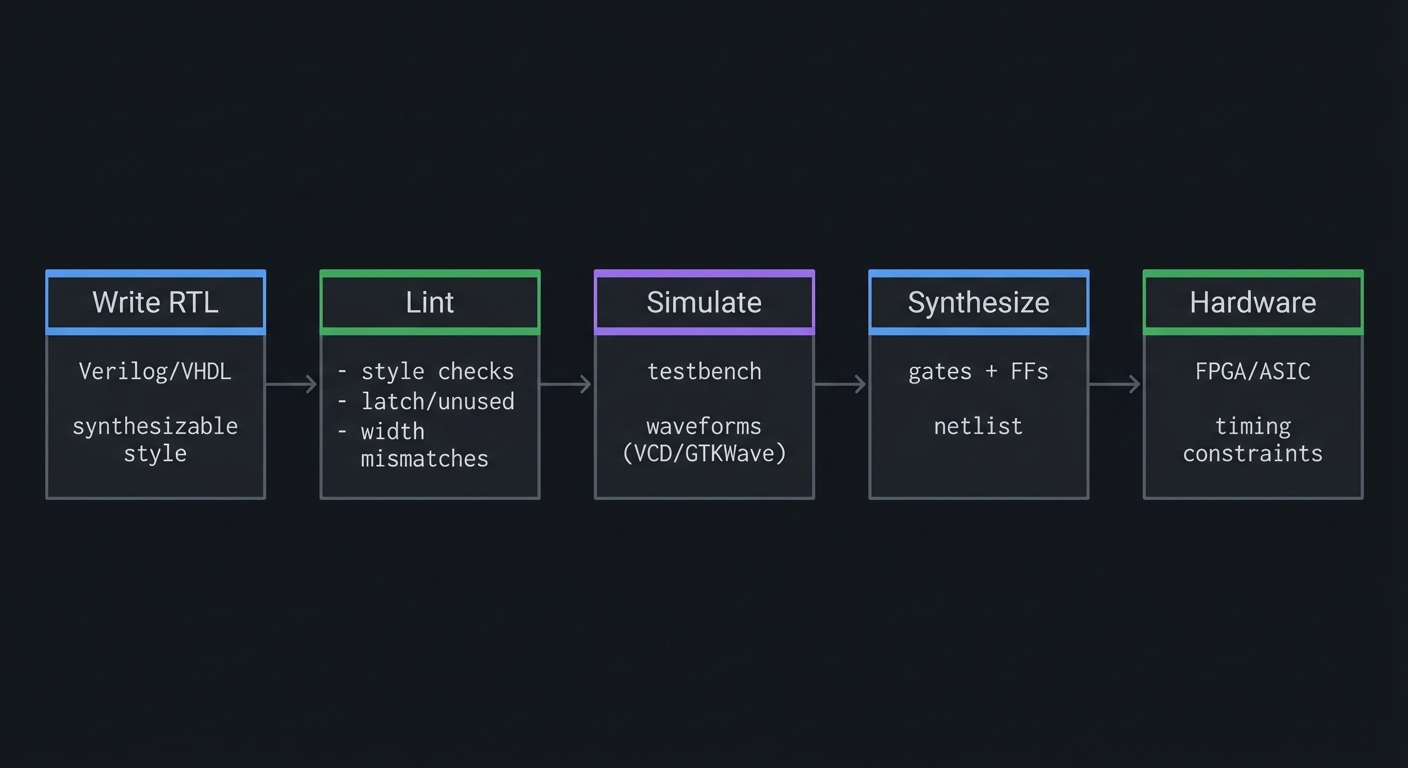
How It Works (Step-by-Step)
- Turn off implicit nets with
`default_nettype none. - Run a linter (e.g., Verilator
-Wall) regularly. - Fix warnings about width mismatches, unused signals, and latches.
- Adopt consistent naming conventions and module boundaries.
Trade-Offs
- Upfront discipline adds time but avoids late-stage hardware bugs.
- Strict linting can be noisy; tune rules to your project.
Minimal Concrete Example
`default_nettype none
module top(input clk, input a, output y);
  wire tmp = a;
  assign y = tmp;
endmodule
`default_nettype wire
Common Misconceptions
- “Warnings are harmless.” (Most HDL bugs start as warnings.)
- “Synthesis will fix it.” (Synthesis can optimize, not correct intent.)
Check-Your-Understanding
- Why is
default_nettype noneuseful? - How can width mismatches create silent bugs?
- What is your project’s naming convention?
Where You’ll Apply It
All projects, especially larger ones (15-20, Final CPU).
Glossary (High-Signal)
- ALU: Arithmetic Logic Unit.
- Blocking assignment:
=inside procedural blocks. - Non-blocking assignment:
<=for clocked logic. - Combinational logic: Outputs depend only on inputs.
- Sequential logic: Outputs depend on state and inputs.
- Clock domain: Logic driven by a single clock.
- Critical path: Longest delay path limiting max frequency.
- FSM: Finite state machine.
- Metastability: Unstable state from async sampling.
- Synchronizer: Chain of flip-flops to reduce metastability risk.
- CDC: Clock domain crossing between unrelated clocks.
- Delta cycle: Zero-time simulation step to settle logic.
- Event queue: Ordered simulation regions that schedule updates.
- Synthesis: Converting RTL to gate-level netlist.
- Constraint (SDC/XDC): Timing or I/O rule for STA.
- STA: Static timing analysis of setup/hold.
- LUT: FPGA lookup table implementing logic.
- Carry chain: Fast adder hardware in FPGA fabric.
- BRAM: Block RAM embedded in FPGA fabric.
- DSP slice: Dedicated multiplier/accumulator block.
- Clock enable: Conditional register update without gating the clock.
- Gray code: Encoding where only one bit changes between values.
- Synthesizable: Can be converted into hardware.
- Testbench: Simulation-only verification module.
- VCD/FST: Waveform dump files.
- Signed/Unsigned: Two’s complement vs pure magnitude interpretation.
- Overflow: Result outside representable signed range.
- Fixed-point (Q format): Integer representation of fractional values.
- Parameter: Compile-time constant for scalable modules.
- Generate: Compile-time replication of hardware.
- Pipeline: Registers inserted to increase max clock speed.
- Latency: Cycles from input to output in a pipeline.
- Throughput: Results produced per cycle once pipeline is full.
- Ready/Valid: Handshake signals to move data safely between modules.
- Backpressure: Consumer throttles producer to prevent overflow.
- Assertion: Property that must always hold.
- Formal verification: Automated proof/exhaustive search of RTL properties.
- Linting: Static analysis for HDL style and correctness issues.
- Implicit net: Undeclared wire created by a typo.
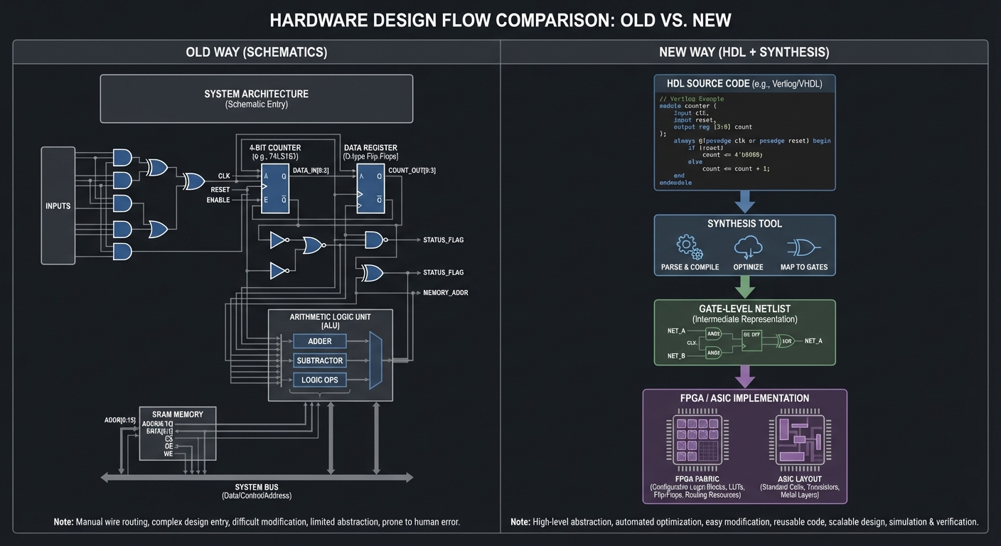
Why Verilog Matters
The Modern Problem It Solves
Verilog lets you scale from a few gates to millions of flip-flops without drawing schematics. It is the language of digital intent: you describe structure + behavior, and tools synthesize it into real hardware. This matters because modern systems require custom acceleration, deterministic latency, and low power, all of which are difficult to achieve in software alone.
Modern Use Cases (Where Verilog Powers Real Systems)
- Data-center acceleration (AI inference, networking offload, storage controllers)
- Low-latency finance and telecom (packet processing, 5G/6G radio)
- Automotive and aerospace (sensor fusion, safety controllers, avionics)
- Robotics and embedded control (motor control, timing-critical sensors)
- Rapid prototyping and ASIC pre-silicon validation
Industry Context (With Sources)
- FPGA market growth: projected to grow from ~USD 11.73B (2025) to ~USD 19.34B by 2030, ~10.5% CAGR (MarketsandMarkets, 2025).
- Standardization: SystemVerilog is standardized as IEEE 1800-2023 (published Feb 28, 2024).
- Adoption: Accellera reports SystemVerilog is used in over 75% of electronic designs (2024).
Context & Evolution (Short)
- 1980s: Verilog emerges for simulation and RTL design.
- 2000s: Verilog and SystemVerilog unify under IEEE 1800 standardization.
- 2020s: Open-source FPGA flows + cloud hardware make RTL skills accessible to individuals.
Old Way (schematics)                New Way (HDL + synthesis)
[gate drawings + manual wiring]     Verilog -> Synthesis -> PnR -> FPGA
Concept Summary Table
| Concept Cluster | What You Must Internalize |
|---|---|
| HDL Mindset | Verilog describes circuits, not instruction sequences. |
| Modules & Hierarchy | Systems are composed of reusable blocks with clear interfaces. |
| Signals & Types | Wires are connections, regs are procedural variables, X/Z exist in simulation. |
| Combinational Logic | assign and always @(*) create pure logic and MUXes. |
| Sequential Logic | always @(posedge clk) + non-blocking assignments create flip-flops. |
| Resets & Safe Clocking | Reset strategy, clock enable usage, safe deassertion. |
| Simulation Semantics | Delta cycles and event queues explain race conditions. |
| Synthesizable Subset | Not all constructs map to hardware; code style matters. |
| CDC & Metastability | Async inputs need synchronizers and careful crossing. |
| FSMs | State encoding, transitions, and output logic drive controllers. |
| Datapaths & Memory | RAM inference and ALU structure build processors. |
| Signed Arithmetic & Fixed-Point | Overflow, sign extension, and numeric formats are explicit in RTL. |
| Parameterization & Generate | Reusable, scalable modules are built with parameters and generate loops. |
| Pipelining & Throughput | Throughput vs latency trade-offs drive performance decisions. |
| Handshakes & Streaming | Ready/valid style protocols prevent data loss under backpressure. |
| Verification | Self-checking testbenches and waveforms are your debugger. |
| Formal Verification | Assertions + bounded proofs catch bugs simulation misses. |
| Constraints & STA | Timing constraints define whether hardware is safe. |
| FPGA Architecture | LUTs, carry chains, BRAM, and DSP blocks matter. |
| Interfaces | UART/SPI/PWM/VGA require strict timing and framing. |
| Debugging | Waveforms + probes are the hardware engineer’s microscope. |
| Linting & Code Hygiene | Warnings and style issues prevent synthesis/sim mismatches. |
Project-to-Concept Map
| Project | Key Concepts |
|---|---|
| 1. Gate Library | HDL mindset, signals/types, combinational logic, simulation semantics, linting/testbench basics |
| 2. 4-to-1 MUX | Combinational logic, case/defaults, latch avoidance, parameterization (optional) |
| 3. 7-Segment Decoder | Encoding, combinational logic, active-high vs active-low, parameterization |
| 4. Ripple Carry Adder | Arithmetic logic, hierarchy, carry propagation, timing |
| 5. 8-bit ALU | Datapath/control, op selection, flags, signed arithmetic, verification |
| 6. D Flip-Flop | Sequential logic, resets, clock enable |
| 7. Counter | Sequential logic, enable/priority, wraparound behavior |
| 8. LED Chaser | Shift registers, timing, clock enables, parameterized width |
| 9. Debouncer | Metastability, CDC patterns, filtering, edge detection |
| 10. PWM Generator | Counters, duty cycle, resolution vs frequency |
| 11. Traffic Light | FSMs, timers, Moore outputs |
| 12. Vending Machine | FSM + datapath + handshakes (dispense pulse) |
| 13. Pattern Detector | FSMs, streaming data, overlap handling |
| 14. Simple RAM | Memory inference, synchronous read/write, latency |
| 15. UART TX | UART framing, baud generator, ready/busy handshake |
| 16. UART RX | Oversampling, mid-bit sampling, CDC considerations |
| 17. SPI Master | CPOL/CPHA modes, shift registers, clocking |
| 18. VGA Patterns | Video timing, counters, constraints, throughput |
| 19. Calculator | FSM + datapath, signed arithmetic, display multiplexing |
| 20. Pong | VGA + game FSM + collision logic + frame pipeline |
| Final CPU | All concepts + constraints + verification (incl. optional formal + pipelining) |
Deep Dive Reading by Concept
| Concept | Book | Chapter |
|---|---|---|
| HDL fundamentals | Digital Design and Computer Architecture, 2nd Ed | Ch. 4 |
| Combinational logic | Digital Design and Computer Architecture, 2nd Ed | Ch. 2 |
| Sequential logic | Digital Design and Computer Architecture, 2nd Ed | Ch. 3 |
| FSMs | Digital Design and Computer Architecture, 2nd Ed | Ch. 3.4 |
| Timing and hazards | Digital Design and Computer Architecture, 2nd Ed | Ch. 3 |
| Signed arithmetic & number systems | Code (Petzold) | Ch. 10-13 |
| Datapaths & ALUs | Digital Design and Computer Architecture, 2nd Ed | Ch. 5 |
| Memory systems | Digital Design and Computer Architecture, 2nd Ed | Ch. 5 |
| CPU design | Digital Design and Computer Architecture, 2nd Ed | Ch. 6-7 |
| ISA concepts | Computer Organization and Design (RISC-V) | Ch. 2 |
| Performance, pipelining, throughput | Computer Architecture (Hennessy & Patterson) | Ch. 1-2 |
| Embedded timing & protocols | Making Embedded Systems, 2nd Ed | Ch. 8-10 |
| Debugging mindset | The Art of Debugging with GDB, DDD, and Eclipse | Ch. 1-3 |
| Graphics basics | Computer Graphics from Scratch | Ch. 1-2 |
Quick Start Guide: First 48 Hours
Day 1: Install tools + first simulation
# macOS
brew install icarus-verilog gtkwave

# Ubuntu/Debian
sudo apt install iverilog gtkwave
Write a simple AND gate and testbench, run iverilog, then open the waveform in GTKWave.
Day 2: First combinational module
Build a 4-to-1 MUX and verify with a testbench. You should be able to predict waveforms before you open GTKWave.
Day 3 (Optional): First synthesis run
Use Yosys to synthesize a tiny design and inspect the netlist. This is your first look at how RTL turns into gates.
Recommended Learning Paths
Path A: Absolute Beginner
- Projects 1-3
- Read DDCA Ch. 2-3
- Projects 6-7
- Get FPGA hardware
- Projects 8-11
Path B: Software Engineer
- Projects 2-5
- Projects 6-7
- Project 11 (FSM)
- Projects 15-16 (UART)
- Final CPU
Path C: Hardware Engineer
- Skim Projects 1-3
- Projects 4-7
- Projects 11-13
- Projects 18-20
- Final CPU
Path D: Fast Hardware Bring-Up
- Projects 1-7 (simulation only)
- Projects 8-10 on FPGA
- Add constraints + timing checks
- Projects 15-18 (protocols + VGA)
- Final CPU
Success Metrics
By the end, you can:
- Explain blocking vs non-blocking and use them correctly.
- Debug timing issues with waveforms and constraints.
- Implement UART, SPI, PWM, and VGA from scratch.
- Explain CDC patterns and where they apply.
- Close timing on a small FPGA design.
- Build a CPU that runs assembly code.
- Explain signed overflow vs carry and implement fixed-point math.
- Use assertions or simple formal checks on key modules.
- Maintain lint-clean RTL with consistent style.
Optional Appendices
Appendix A: Toolchain Cheat Sheet
# Simulate
iverilog -o sim top.v tb.v
vvp sim

# View waveforms
gtkwave dump.vcd
Appendix B: Common Synthesis Pitfalls
- Using delays (
#10) in synthesizable code - Incomplete sensitivity lists
- Implicit latches from missing assignments
- Mixing blocking and non-blocking in sequential blocks
Appendix C: Reset and CDC Checklist
- Use one reset strategy consistently (sync or async)
- Synchronize async inputs with 2+ flip-flops
- Avoid combinational logic between synchronizer flops
- Constrain clocks properly in your SDC/XDC
Appendix D: VGA 640x480@60 Timing (Reference)
Active: 640 x 480
Front porch: 16 (H) / 10 (V)
Sync: 96 (H) / 2 (V)
Back porch: 48 (H) / 33 (V)
Total: 800 x 525
Sync polarity: negative (H/V)
Pixel clock: 25.175 MHz nominal (25.2 MHz is commonly used)
Appendix E: Minimal SDC Template
create_clock -name clk -period 20 [get_ports clk]
set_input_delay 2 -clock clk [get_ports rx]
set_output_delay 2 -clock clk [get_ports tx]
Appendix F: CDC Patterns Quick Reference
Single-bit level   -> 2-FF synchronizer
Pulse              -> toggle sync or handshake
Multi-bit bus      -> async FIFO (Gray pointers)
Appendix G: Open-Source FPGA Flow (iCE40 + ECP5)
# iCE40 flow
yosys -p "synth_ice40 -json top.json" top.v
nextpnr-ice40 --hx8k --json top.json --asc top.asc
icepack top.asc top.bin
iceprog top.bin

# ECP5 flow (ULX3S)
yosys -p "synth_ecp5 -json top.json" top.v
nextpnr-ecp5 --25k --json top.json --textcfg top.config
ecppack top.config top.bit
Appendix H: Minimal SymbiYosys (Formal) Template
[options]
mode bmc
depth 20

[engines]
smtbmc

[script]
read -formal top.v
prep -top top

[files]
top.v
Appendix I: Linting Quick Start (Verilator)
verilator -Wall --lint-only top.v
Appendix J: Waveform Formats (VCD vs FST)
- VCD is the standard, human-readable waveform dump.
- FST is a compact, faster-to-load format for large simulations.
- GTKWave can open both VCD and FST, so you can switch formats as designs grow.
Projects
Project 1: Digital Gate Library
- Main Programming Language: Verilog
- Alternative Programming Languages: VHDL, SystemVerilog
- Difficulty: Beginner
- Time Estimate: 2-3 hours
- Knowledge Area: Combinational Logic
- Main Book: Digital Design and Computer Architecture, 2nd Ed
What you’ll build: AND, OR, NOT, XOR, NAND, NOR modules plus a testbench that proves correctness for all input combinations.
Why it teaches Verilog: This is your “hello world” in hardware. You learn module ports, continuous assignments, and waveforms.
Core challenges:
- Mapping truth tables to continuous assignments
- Writing testbenches that cover all input combinations
Real World Outcome
$ iverilog -o gates_tb gates.v gates_tb.v
$ vvp gates_tb
PASS: AND
PASS: OR
PASS: XOR
PASS: NAND
PASS: NOR
PASS: NOT

$ gtkwave gates.vcd
# You see clean transitions for every input pair and no X after init.
The Core Question You’re Answering
“How do I translate a truth table into hardware that always behaves correctly?”
Concepts You Must Understand First
- Truth tables and Boolean algebra (DDCA Ch. 2)
- Continuous assignments (DDCA Ch. 4)
- Testbench basics and VCD dumps (DDCA Ch. 4)
Questions to Guide Your Design
- Are all input combinations tested?
- Is every output driven for every case?
- Do your outputs ever go X due to missing initialization?
Thinking Exercise
Write the XOR truth table and mark which inputs yield 1. Then sketch how XOR can be built from AND/OR/NOT.
The Interview Questions They’ll Ask
- What is the difference between a wire and a reg?
- What hardware does
assigninfer? - How do you test all input combinations?
- What is a testbench and why is it separate from the DUT?
Hints in Layers
- Implement AND/OR/NOT first.
- Build XOR from AND/OR/NOT or use the
^operator. - Use a
forloop to iterate inputs in the testbench.
assign and_out = a & b;
integer i;
initial begin
  for (i = 0; i < 4; i = i + 1) begin
    {a,b} = i; #1;
  end
end
Implementation Plan (Suggested)
- Create separate modules for AND, OR, XOR, NAND, NOR, NOT.
- Keep port names consistent across all gate modules.
- (Optional) Create a
gates_topmodule that instantiates all gates for easier probing. - Write a testbench that iterates all input combinations and checks expected outputs.
Verification Plan
- Exhaustively test all input combinations for each gate.
- Use self-checking assertions or explicit PASS/FAIL messages.
- Verify waveforms have no lingering X after initialization.
Books That Will Help
| Topic | Book | Chapter | |——|——|———| | Boolean logic | DDCA | Ch. 2 | | Verilog basics | DDCA | Ch. 4 |
Common Pitfalls & Debugging
Problem: Outputs stay X
- Why: Undriven wires or missing assignments.
- Fix: Ensure every output has a driver.
- Quick test: Run
vvp gates_tband verify all PASS lines.
Problem: Testbench never finishes
- Why: Missing
$finish. - Fix: Add a final
$finishafter your stimulus loop. - Quick test: Confirm the simulator exits with code 0.
Definition of Done
- All six gates pass exhaustive test vectors
- Waveforms show no X after initialization
- Testbench terminates cleanly with
$finish
Project 2: 4-to-1 Multiplexer
- Main Programming Language: Verilog
- Difficulty: Beginner
- Time Estimate: 2-3 hours
- Knowledge Area: Combinational Logic
What you’ll build: A 4-to-1 MUX with select lines and a testbench.
Real World Outcome
$ vvp mux_tb
sel=00 -> y=a
sel=01 -> y=b
sel=10 -> y=c
sel=11 -> y=d

$ gtkwave mux.vcd
# You see y tracking the selected input with no glitches.
The Core Question You’re Answering
“How does hardware choose one signal from many?”
Concepts You Must Understand First
- Combinational logic blocks (
always @(*)) - DDCA Ch. 2 - Case statements and defaults - DDCA Ch. 4
- Latch avoidance (all paths assigned)
Questions to Guide Your Design
- What happens if
selis X or Z? - How do you prevent latch inference?
- How do you test for glitches during select changes?
Thinking Exercise
Sketch a 4-to-1 MUX using only AND/OR gates. Identify the select inversion terms.
The Interview Questions They’ll Ask
- What hardware does an if/else create?
- Why is a default case required?
- What is the difference between a priority mux and a regular mux?
- When does a mux create a combinational loop?
Hints in Layers
- Write a
case (sel)block and assignyin all branches. - Add a
defaultthat assignsyto a safe value. - In the testbench, iterate
selacross all values.
always @(*) begin
  case (sel)
    2'b00: y = a;
    2'b01: y = b;
    2'b10: y = c;
    default: y = d;
  endcase
end
Implementation Plan (Suggested)
- Define inputs
a,b,c,dandsel[1:0], outputy. - Use a
casestatement with a default to cover all select values. - (Optional) Parameterize data width (e.g.,
parameter W=1). - Build a testbench that assigns distinct patterns to each input and sweeps
sel.
Verification Plan
- For each
sel, assertymatches the correct input. - Toggle input values while
selis stable to check propagation. - Test
selunknowns (X/Z) and confirm default behavior.
Books That Will Help
| Topic | Book | Chapter | |——|——|———| | Muxes and combinational logic | DDCA | Ch. 2 | | Verilog case statements | DDCA | Ch. 4 |
Common Pitfalls & Debugging
Problem: Latch inferred
- Why: Missing assignment in a branch.
- Fix: Assign
yin all branches or set a default first. - Quick test: Inspect synthesis warnings or check waveforms for held values.
Definition of Done
- All four select cases work
- No latch inference warnings
- Waveforms show correct routing on select changes
Project 3: 7-Segment Display Decoder
- Main Programming Language: Verilog
- Difficulty: Beginner
- Time Estimate: 3-4 hours
- Knowledge Area: Encoding / Combinational Logic
What you’ll build: A hex-to-7-seg decoder (0-F) and testbench. Optional: drive a real 7-seg display.
Real World Outcome
$ vvp seg7_tb
0 -> 0b0111111
1 -> 0b0000110
A -> 0b1110111
F -> 0b1110001

$ gtkwave seg7.vcd
# Each input nibble maps to the correct segment pattern.
The Core Question You’re Answering
“How do you map symbolic values to physical LED segments?”
Concepts You Must Understand First
- Truth tables and encoding (DDCA Ch. 2)
- Combinational case statements (DDCA Ch. 4)
- Active-high vs active-low outputs
Questions to Guide Your Design
- Are your segments active-high or active-low?
- Will you support hex (0-F) or only decimal (0-9)?
- How will you test all 16 input combinations?
Thinking Exercise
Draw a 7-seg display and label segments A-G. Write which segments must be ON for “A” and “F”.
The Interview Questions They’ll Ask
- Why do some 7-seg displays use active-low signals?
- How do you avoid magic numbers in a decoder?
- How would you extend this to multiple digits?
- What is segment multiplexing?
Hints in Layers
- Start with a lookup table using
case. - Use a named parameter for each segment bit.
- Write a testbench that loops through 0-15.
always @(*) begin
  case (hex)
    4'h0: seg = 7'b0111111;
    4'h1: seg = 7'b0000110;
    4'hA: seg = 7'b1110111;
    default: seg = 7'b0000000;
  endcase
end
Implementation Plan (Suggested)
- Choose a segment bit order (A-G) and document it clearly.
- Decide active-high vs active-low and encode patterns accordingly.
- Implement a combinational
casefor 0-F. - (Optional) Add a parameter to invert outputs for active-low hardware.
Verification Plan
- Exhaustively test all 16 input values.
- Compare outputs to a known 7-seg truth table.
- If using hardware, light each segment individually to confirm wiring order.
Books That Will Help
| Topic | Book | Chapter | |——|——|———| | Encoding and logic | DDCA | Ch. 2 | | Verilog case tables | DDCA | Ch. 4 |
Common Pitfalls & Debugging
Problem: Digits appear mirrored
- Why: Segment wiring order doesn’t match bit order.
- Fix: Re-map bits to match your physical display.
- Quick test: Light each segment individually.
Definition of Done
- All 16 hex inputs map correctly
- Testbench covers every input
- Segment polarity documented (active-high/low)
Project 4: 4-bit Ripple Carry Adder
- Main Programming Language: Verilog
- Difficulty: Beginner-Intermediate
- Time Estimate: 4-5 hours
- Knowledge Area: Arithmetic Logic
What you’ll build: A 4-bit ripple-carry adder using full adders and a testbench.
Real World Outcome
$ vvp adder_tb
3 + 5 = 8 (carry=0)
9 + 7 = 0 (carry=1)
15 + 1 = 0 (carry=1)

$ gtkwave adder.vcd
# You can see carry propagate bit-by-bit.
The Core Question You’re Answering
“Why does carry ripple, and how does that affect timing?”
Concepts You Must Understand First
- Full adder logic (DDCA Ch. 2)
- Ripple-carry timing and propagation delay
- Module hierarchy (DDCA Ch. 4)
Questions to Guide Your Design
- Do you want a structural (full-adder chain) or behavioral add?
- How will you expose carry-out?
- How will you verify overflow?
Thinking Exercise
Draw the chain of 4 full adders and label each carry output. Which bit is the critical path?
The Interview Questions They’ll Ask
- Why is ripple carry slower than carry-lookahead?
- What is the critical path in a ripple adder?
- How do you detect overflow for signed vs unsigned?
- When is a behavioral
+ok in RTL?
Hints in Layers
- Write a 1-bit full adder module.
- Chain 4 full adders with carry connections.
- Test with vectors that force long carry chains.
assign {c_out, sum} = a + b + c_in; // behavioral full adder
Implementation Plan (Suggested)
- Implement a 1-bit full adder module (sum + carry).
- Chain four full adders with carry propagation.
- Expose both sum[3:0] and carry-out.
- Create a testbench that checks normal and carry-heavy cases.
Verification Plan
- Exhaustively test all 256 input pairs.
- Include directed tests like
0xF + 0x1and0x8 + 0x8. - Inspect waveforms to see carry ripple through each bit.
Books That Will Help
| Topic | Book | Chapter | |——|——|———| | Adders | DDCA | Ch. 2 | | Structural design | DDCA | Ch. 4 |
Common Pitfalls & Debugging
Problem: Wrong carry-out
- Why: Carry chain wired incorrectly.
- Fix: Check that each carry connects to the next stage.
- Quick test: Add 0xF + 0x1 and expect carry=1.
Definition of Done
- Sum and carry are correct for all 256 input pairs
- Carry chain is visible and correct in waveforms
Project 5: 8-bit ALU (Arithmetic Logic Unit)
- Main Programming Language: Verilog
- Difficulty: Intermediate
- Time Estimate: 1 week
- Knowledge Area: Datapath Design
What you’ll build: An 8-bit ALU supporting add, subtract, AND, OR, XOR, shifts, and flag outputs (Z, C, N).
Real World Outcome
$ vvp alu_tb
OP=ADD  0x12 + 0x34 = 0x46  Z=0 C=0 N=0
OP=SUB  0x10 - 0x20 = 0xF0  Z=0 C=1 N=1
OP=AND  0xF0 & 0x0F = 0x00  Z=1 C=0 N=0

$ gtkwave alu.vcd
# Flags change deterministically with each operation.
The Core Question You’re Answering
“How do real CPUs choose arithmetic operations and generate flags?”
Concepts You Must Understand First
- Datapath + control separation (DDCA Ch. 5)
- Add/subtract using two’s complement
- Flag generation (zero, carry, negative)
Questions to Guide Your Design
- How many opcode bits do you need?
- Will shifts be logical or arithmetic?
- How will you define the carry/borrow flag for subtraction?
Thinking Exercise
Define an opcode table for 8 operations and write the expected flags for 0x00 + 0x00, 0xFF + 0x01, and 0x80 - 0x01.
The Interview Questions They’ll Ask
- What does the zero flag represent?
- How do you detect carry vs overflow?
- How do you implement subtraction in hardware?
- Why do CPUs separate datapath and control?
- How would you add comparison operations?
Hints in Layers
- Build add/sub first, then bitwise ops.
- Implement flags as combinational outputs of the result.
- Use a
caseon opcode to select the ALU result.
always @(*) begin
  case (op)
    3'b000: y = a + b;
    3'b001: y = a - b;
    3'b010: y = a & b;
    default: y = 8'h00;
  endcase
end
assign z = (y == 0);
Implementation Plan (Suggested)
- Define a clear opcode table (add, sub, and/or/xor, shifts).
- Use widened arithmetic to compute carry/overflow flags.
- Implement flags Z (zero), N (negative), C (carry/borrow), V (overflow).
- Write a self-checking testbench with a software reference model.
Verification Plan
- Directed edge cases:
0x00,0xFF,0x80,0x01. - Randomized vectors with a golden reference model.
- Validate flag behavior for add and subtract separately.
Books That Will Help
| Topic | Book | Chapter | |——|——|———| | ALU and datapaths | DDCA | Ch. 5 | | Two’s complement | Code (Petzold) | Ch. 12 |
Common Pitfalls & Debugging
Problem: Wrong flags on subtraction
- Why: Borrow vs carry logic confusion.
- Fix: Define flag behavior clearly and test edge cases.
- Quick test:
0x00 - 0x01should set negative and borrow.
Definition of Done
- All operations match the opcode table
- Flags match expected results for edge cases
- Testbench covers random vectors and edge vectors
Project 6: D Flip-Flop (The Building Block of Memory)
- Main Programming Language: Verilog
- Difficulty: Beginner
- Time Estimate: 2-3 hours
- Knowledge Area: Sequential Logic
What you’ll build: A D flip-flop with synchronous reset and enable, plus a testbench.
Real World Outcome
$ vvp dff_tb
t=0 reset=1 q=0
t=10 d=1 en=1 q=1
t=20 d=0 en=0 q=1 (held)

$ gtkwave dff.vcd
# q only updates on clock edges and respects enable.
The Core Question You’re Answering
“How does hardware remember a value from one clock edge to the next?”
Concepts You Must Understand First
- Edge-triggered logic (DDCA Ch. 3)
- Non-blocking assignments
- Reset strategies (sync vs async)
Questions to Guide Your Design
- Do you want a synchronous or asynchronous reset?
- How should enable affect updates?
- What is the output during reset?
Thinking Exercise
Draw a timeline of clk, d, en, reset, and q. Predict q for each clock edge.
The Interview Questions They’ll Ask
- Why use non-blocking assignments in sequential logic?
- What is the difference between latch and flip-flop?
- When would you use async reset?
- What happens if reset deasserts near the clock edge?
Hints in Layers
- Start with
always @(posedge clk). - Add reset logic first, then enable.
- Use a testbench that toggles d between clock edges.
always @(posedge clk) begin
  if (reset) q <= 1'b0;
  else if (en) q <= d;
end
Implementation Plan (Suggested)
- Write a DFF with synchronous reset and enable.
- (Optional) Parameterize width to create N-bit registers.
- Build a testbench that toggles
d,en, andresetacross edges.
Verification Plan
- Confirm
qchanges only on rising clock edges. - Verify reset sets
qdeterministically. - Ensure
qholds value whenen=0.
Books That Will Help
| Topic | Book | Chapter | |——|——|———| | Sequential logic | DDCA | Ch. 3 | | Timing basics | DDCA | Ch. 3 |
Common Pitfalls & Debugging
Problem: q updates without clock edge
- Why: Combinational assignment to q.
- Fix: Move q assignment into a clocked always block.
- Quick test: Check waveforms for updates between edges.
Definition of Done
- q changes only on clock edges
- reset forces q to known value
- enable prevents updates when low
Project 7: 4-bit Up/Down Counter with Load
- Main Programming Language: Verilog
- Difficulty: Intermediate
- Time Estimate: 4-5 hours
- Knowledge Area: Sequential Logic
What you’ll build: A 4-bit counter with up/down control, load, and enable.
Real World Outcome
$ vvp counter_tb
load=1 data=9 -> count=9
up=1 en=1 -> 10,11,12
up=0 en=1 -> 11,10,9

$ gtkwave counter.vcd
# Count changes only on clock edges and respects load/enable.
The Core Question You’re Answering
“How do counters combine state, control, and priority of operations?”
Concepts You Must Understand First
- Sequential logic with enable (DDCA Ch. 3)
- Priority logic in sequential blocks
- Wraparound behavior (modulo arithmetic)
Questions to Guide Your Design
- Which has priority: load or count?
- What happens at 0 or 15 (wraparound)?
- How do you test both up and down modes?
Thinking Exercise
Create a state table for count, up/down, load, and enable. Mark the priority order.
The Interview Questions They’ll Ask
- How do you implement priority in a clocked always block?
- What is modulo arithmetic in hardware?
- How do you avoid double-counting when enable glitches?
- When would you gate a clock vs use enable?
Hints in Layers
- Start with the load case at the top of the if/else chain.
- Add enable gating for counting.
- Use
count <= count + 1'b1orcount - 1'b1.
always @(posedge clk) begin
  if (reset) count <= 0;
  else if (load) count <= data;
  else if (en) count <= up ? count + 1 : count - 1;
end
Implementation Plan (Suggested)
- Define priority: reset > load > count.
- Implement up/down arithmetic with wraparound.
- (Optional) Parameterize width for reusability.
- Test with sequences that toggle load, enable, and direction.
Verification Plan
- Check boundary behavior at 0 and max.
- Verify load always overrides counting.
- Run random sequences and compare to a software counter.
Books That Will Help
| Topic | Book | Chapter | |——|——|———| | Counters | DDCA | Ch. 3 | | Sequential logic | DDCA | Ch. 3 |
Common Pitfalls & Debugging
Problem: Count jumps unexpectedly
- Why: Load and count logic both active without clear priority.
- Fix: Enforce a priority order in the if/else chain.
- Quick test: Toggle load and enable in the same cycle and verify expected result.
Definition of Done
- Count updates only on clock edges
- Load overrides counting
- Up/down directions work and wrap correctly
Project 8: Shift Register LED Chaser
- Main Programming Language: Verilog
- Difficulty: Intermediate
- Time Estimate: 1 weekend
- Knowledge Area: Sequential Logic / Timing
What you’ll build: An 8-bit shift register with a visible LED “chaser” pattern.
Real World Outcome
$ vvp shift_tb
00000001
00000010
00000100
00001000
...

On FPGA: LEDs appear to move left-right at a human-visible rate.
The Core Question You’re Answering
“How do you create visible motion from a fast digital clock?”
Concepts You Must Understand First
- Shift registers (DDCA Ch. 3)
- Clock enable / clock divider
- Reset to a known pattern
Questions to Guide Your Design
- How do you slow the pattern to human-visible speed?
- Should the pattern wrap or bounce?
- How do you avoid all LEDs turning off?
Thinking Exercise
Write the bit pattern for a bouncing LED (left to right, then right to left) for 10 steps.
The Interview Questions They’ll Ask
- What is a shift register used for?
- How do you implement clock enable?
- Why is a clock divider safer than gating the clock?
- How would you change speed at runtime?
Hints in Layers
- Implement an 8-bit register with shift left.
- Add a slow tick using a counter.
- Add direction logic to bounce.
if (tick) begin
  leds <= {leds[6:0], leds[7]};
end
Implementation Plan (Suggested)
- Implement an 8-bit shift register for LED patterns.
- Add a slow tick using a counter divider.
- (Optional) Add direction control for bounce effect.
- Create a testbench that drives ticks and checks patterns.
Verification Plan
- Confirm one-bit “1” moves on each tick.
- Ensure pattern wraps or bounces as intended.
- Verify reset restores a known starting pattern.
Books That Will Help
| Topic | Book | Chapter | |——|——|———| | Shift registers | DDCA | Ch. 3 | | Timing | DDCA | Ch. 3 |
Common Pitfalls & Debugging
Problem: LEDs move too fast
- Why: No clock divider.
- Fix: Use a counter to create a slower enable tick.
- Quick test: Increase divider and confirm visible speed change.
Definition of Done
- Pattern advances only on slow tick
- Reset sets a known initial LED pattern
- No stuck-all-zero state
Project 9: Button Debouncer
- Main Programming Language: Verilog
- Difficulty: Intermediate
- Time Estimate: 4-5 hours
- Knowledge Area: Timing / CDC
What you’ll build: A debouncer that turns noisy button edges into clean pulses.
Real World Outcome
$ vvp debounce_tb
raw:  10111010001111
clean:10000000000001

On FPGA: One clean pulse per button press.
The Core Question You’re Answering
“How do you filter real-world noise before it becomes state?”
Concepts You Must Understand First
- Metastability and synchronizers (DDCA Ch. 3)
- Counter-based filtering
- Edge detection
Questions to Guide Your Design
- How many samples are enough for “stable”?
- Will you output level or pulse?
- How do you handle long presses?
Thinking Exercise
Draw a noisy button waveform and circle which parts should be ignored.
The Interview Questions They’ll Ask
- Why is a synchronizer needed for a button?
- How does a counter-based debouncer work?
- What is the trade-off between responsiveness and filtering?
- How would you debounce multiple buttons?
Hints in Layers
- Synchronize the raw button with two flip-flops.
- Use a counter that increments while the input is stable.
- Output a pulse on a clean rising edge.
if (sync_btn == stable_btn) count <= 0;
else count <= count + 1;
if (count == MAX) stable_btn <= sync_btn;
Implementation Plan (Suggested)
- Synchronize the raw button input with a 2-FF chain.
- Use a counter to detect stable levels across N cycles.
- Add edge detection to generate a clean pulse.
- Parameterize debounce time for different clocks.
Verification Plan
- Simulate noisy bounce patterns and verify one output pulse.
- Hold the button and confirm no repeated pulses (unless desired).
- Verify reset clears internal state cleanly.
Books That Will Help
| Topic | Book | Chapter | |——|——|———| | Synchronizers | DDCA | Ch. 3 | | Timing/CDC | DDCA | Ch. 3 |
Common Pitfalls & Debugging
Problem: Multiple pulses per press
- Why: Edge detection on the raw signal.
- Fix: Detect edges on the debounced signal only.
- Quick test: Hold the button down and confirm only one pulse.
Definition of Done
- One clean pulse per press
- No response to bounce noise
- Works across repeated presses
Project 10: PWM Generator (LED Dimmer / Servo Control)
- Main Programming Language: Verilog
- Difficulty: Intermediate
- Time Estimate: 4-6 hours
- Knowledge Area: Counters / Timing
What you’ll build: A PWM generator with configurable duty cycle. Optional: drive an LED or servo.
Real World Outcome
$ vvp pwm_tb
Duty=10% -> pulse width 1/10 period
Duty=50% -> pulse width 5/10 period
Duty=90% -> pulse width 9/10 period

On FPGA: LED brightness changes smoothly with duty.
The Core Question You’re Answering
“How can a digital signal emulate analog behavior?”
Concepts You Must Understand First
- Counters and comparators (DDCA Ch. 3)
- Duty cycle and resolution
- Clock enable / prescaling
Questions to Guide Your Design
- What PWM resolution (8-bit, 10-bit) do you need?
- What PWM frequency works for LEDs vs servos?
- How will you avoid glitches when duty changes?
Thinking Exercise
Calculate the PWM period for a 50 MHz clock and 8-bit counter. Is that OK for LED dimming?
The Interview Questions They’ll Ask
- What is duty cycle?
- How does PWM create analog-like output?
- How do you trade frequency vs resolution?
- Why do servos need about 50 Hz PWM?
Hints in Layers
- Use a free-running counter.
- Compare the counter to a duty register.
- Output high when counter < duty.
pwm_out <= (counter < duty);
Implementation Plan (Suggested)
- Create a free-running counter for PWM period.
- Compare counter to a duty register to generate the PWM output.
- (Optional) Register duty updates to avoid glitches mid-period.
- Parameterize resolution and frequency (counter width).
Verification Plan
- Measure high-time ratio in cycles vs expected duty.
- Sweep duty values (0%, 50%, 100%).
- Confirm PWM frequency matches configuration.
Books That Will Help
| Topic | Book | Chapter | |——|——|———| | Counters | DDCA | Ch. 3 | | Embedded timing | Making Embedded Systems | Ch. 8 |
Common Pitfalls & Debugging
Problem: LED flickers
- Why: PWM frequency too low.
- Fix: Increase counter clock or reduce counter width.
- Quick test: Raise frequency and observe flicker reduction.
Definition of Done
- Output duty matches configured value
- PWM frequency within expected range
- Duty updates without glitches
Project 11: Traffic Light Controller
- Main Programming Language: Verilog
- Difficulty: Intermediate
- Time Estimate: 1 weekend
- Knowledge Area: FSMs
What you’ll build: A traffic light FSM with timed phases and safe transitions.
Real World Outcome
$ vvp traffic_tb
STATE=GREEN  t=0..29
STATE=YELLOW t=30..34
STATE=RED    t=35..64

On FPGA: LEDs cycle green-yellow-red in correct order.
The Core Question You’re Answering
“How do you model timed real-world behavior with finite state machines?”
Concepts You Must Understand First
- FSM encoding (DDCA Ch. 3.4)
- Timers and counters
- Output decoding from state
Questions to Guide Your Design
- How long should each state last?
- Do you need a yellow phase before red?
- How do you ensure only valid transitions occur?
Thinking Exercise
Draw a state diagram and label each transition with time or condition.
The Interview Questions They’ll Ask
- Moore vs Mealy: which is safer for traffic lights?
- How do you implement timed transitions?
- How would you add a pedestrian crossing button?
- What is one-hot encoding and why use it?
Hints in Layers
- Define states: GREEN, YELLOW, RED.
- Use a timer counter to trigger transitions.
- Map outputs from state (Moore style).
case (state)
  GREEN:  if (timer_done) state <= YELLOW;
  YELLOW: if (timer_done) state <= RED;
  RED:    if (timer_done) state <= GREEN;
endcase
Implementation Plan (Suggested)
- Define FSM states (GREEN, YELLOW, RED).
- Implement a timer/counter for state duration.
- Drive outputs based on state (Moore style).
- Build a testbench that runs multiple full cycles.
Verification Plan
- Verify correct order and timing per state.
- Ensure no illegal transitions occur.
- Confirm output stability within each state window.
Books That Will Help
| Topic | Book | Chapter | |——|——|———| | FSMs | DDCA | Ch. 3.4 | | Timers | Making Embedded Systems | Ch. 8 |
Common Pitfalls & Debugging
Problem: Skipped states
- Why: Timer resets incorrectly on transitions.
- Fix: Reset timer when state changes.
- Quick test: Force long simulation and confirm full cycle order.
Definition of Done
- Correct sequence and timing of lights
- No illegal state transitions
- Outputs are stable within each state
Project 12: Vending Machine Controller
- Main Programming Language: Verilog
- Difficulty: Advanced
- Time Estimate: 1 week
- Knowledge Area: FSMs + Datapath
What you’ll build: A vending machine FSM that accepts coins, tracks balance, and dispenses products.
Real World Outcome
$ vvp vending_tb
coin=25 -> balance=25
coin=25 -> balance=50
select=1 -> DISPENSE
change=0

On FPGA: LEDs show balance and dispense signal pulses when paid.
The Core Question You’re Answering
“How do you combine control (FSM) with data (balance and pricing)?”
Concepts You Must Understand First
- FSM design (DDCA Ch. 3.4)
- Datapath registers and comparators
- Output pulses and handshaking
Questions to Guide Your Design
- What coin denominations are supported?
- How do you handle overpayment and change?
- How do you prevent double-dispense?
Thinking Exercise
Write the state transitions for inserting a coin, selecting a product, and dispensing.
The Interview Questions They’ll Ask
- How do you avoid glitches when asserting DISPENSE?
- Moore vs Mealy for vending logic?
- How do you store and compare balance in hardware?
- How would you add multiple products?
Hints in Layers
- Separate the FSM (control) from balance register (datapath).
- Use a comparator
balance >= price. - Generate a one-cycle DISPENSE pulse.
if (dispense) balance <= balance - price;
Implementation Plan (Suggested)
- Implement a balance register that adds coin values.
- Use a comparator for
balance >= price. - FSM controls idle, accept, dispense, and change states.
- Generate a one-cycle DISPENSE pulse on valid purchase.
Verification Plan
- Test exact payment, overpayment, and multiple coins.
- Hold select high and ensure only one dispense.
- Verify balance updates correctly after dispense/change.
Books That Will Help
| Topic | Book | Chapter | |——|——|———| | FSMs | DDCA | Ch. 3.4 | | Datapaths | DDCA | Ch. 5 |
Common Pitfalls & Debugging
Problem: Dispense repeats
- Why: DISPENSE signal stays high for multiple cycles.
- Fix: Generate a single-cycle pulse on transition.
- Quick test: Hold select high and verify only one dispense.
Definition of Done
- Accepts coins and tracks balance
- Dispense occurs exactly once per purchase
- Balance updates correctly after dispense
Project 13: Serial Pattern Detector (Find 10110)
- Main Programming Language: Verilog
- Difficulty: Advanced
- Time Estimate: 1 weekend
- Knowledge Area: FSMs / Streaming Data
What you’ll build: A Mealy or Moore FSM that asserts match when it detects the bit pattern 10110 in a serial stream.
Real World Outcome
$ vvp pattern_tb
stream=110101101001
match pulses at bit index 6

$ gtkwave pattern.vcd
# match is a single-cycle pulse at the correct position.
The Core Question You’re Answering
“How does hardware recognize patterns in a live data stream?”
Concepts You Must Understand First
- FSMs for pattern detection
- Overlapping matches
- Serial input timing
Questions to Guide Your Design
- Will you allow overlapping matches?
- Moore or Mealy output?
- How do you handle reset mid-stream?
Thinking Exercise
Draw the state diagram for detecting 10110 with overlaps. Label transitions.
The Interview Questions They’ll Ask
- What is the difference between Moore and Mealy for pattern detectors?
- How do you handle overlapping patterns?
- Why does the output sometimes assert one cycle earlier in Mealy?
- How do you test a streaming FSM?
Hints in Layers
- Write states for partial matches (1,10,101,1011,10110).
- Decide overlap rules and adjust transitions.
- Output match when you hit the final state.
if (state == S_1011 && in_bit) match = 1'b1;
Implementation Plan (Suggested)
- Define states for partial matches (1, 10, 101, 1011).
- Choose Mealy or Moore output and implement transitions.
- Add overlap handling to avoid missing patterns.
- Build a streaming testbench with known match positions.
Verification Plan
- Verify detection on overlapping stream (e.g., 10110110).
- Check reset mid-stream returns to IDLE.
- Use a scoreboard to confirm match positions.
Books That Will Help
| Topic | Book | Chapter | |——|——|———| | FSMs | DDCA | Ch. 3.4 | | Sequential logic | DDCA | Ch. 3 |
Common Pitfalls & Debugging
Problem: Missed overlapping matches
- Why: Transitions reset to IDLE instead of partial match.
- Fix: Use overlap-aware transitions.
- Quick test: Stream
10110110and expect two matches.
Definition of Done
- Correct detection with and without overlap
- match is exactly one cycle
- Reset clears internal state
Project 14: Simple RAM (8 words x 8 bits)
- Main Programming Language: Verilog
- Difficulty: Intermediate
- Time Estimate: 3-4 hours
- Knowledge Area: Memory Inference
What you’ll build: An 8x8 RAM with synchronous write and read behavior.
Real World Outcome
$ vvp ram_tb
write addr=3 data=0xAA
write addr=4 data=0x55
read  addr=3 -> 0xAA
read  addr=4 -> 0x55
The Core Question You’re Answering
“How do you model memory so synthesis infers real RAM blocks?”
Concepts You Must Understand First
- Memory arrays in Verilog
- Synchronous vs asynchronous read
- Write enable timing
Questions to Guide Your Design
- Will reads be synchronous or async?
- What happens on read-during-write?
- How will you initialize memory for simulation?
Thinking Exercise
Write a truth table for we and addr showing how dout should behave.
The Interview Questions They’ll Ask
- Why do FPGA BRAMs prefer synchronous reads?
- What is read-during-write behavior?
- How do you infer block RAM vs flip-flops?
- How do you initialize memory in simulation?
Hints in Layers
- Use a
reg [7:0] mem [0:7]array. - In a clocked block, write when
weis high. - Assign
douton clock edge for synchronous read.
always @(posedge clk) begin
  if (we) mem[addr] <= din;
  dout <= mem[addr];
end
Implementation Plan (Suggested)
- Declare a
regarray for memory storage. - Implement synchronous write on
posedge clk. - Define synchronous read behavior (document 1-cycle latency).
- Initialize memory for simulation if needed.
Verification Plan
- Write/read all addresses and compare to expected.
- Test read-during-write behavior explicitly.
- Confirm output latency matches documentation.
Books That Will Help
| Topic | Book | Chapter | |——|——|———| | Memory | DDCA | Ch. 5 | | Sequential logic | DDCA | Ch. 3 |
Common Pitfalls & Debugging
Problem: Read data is one cycle late
- Why: Synchronous read behavior.
- Fix: Document latency and test for it.
- Quick test: Read after a known write and expect a one-cycle delay.
Definition of Done
- Correct reads and writes across all addresses
- Documented read latency
- Testbench covers read-during-write case
Project 15: UART Transmitter
- Main Programming Language: Verilog
- Difficulty: Advanced
- Time Estimate: 1 week
- Knowledge Area: Serial Protocols
What you’ll build: A UART TX module that sends 8N1 frames at a configurable baud rate.
Real World Outcome
$ vvp uart_tx_tb
TX byte=0x55
frame: start(0) 01010101 stop(1)

$ gtkwave uart_tx.vcd
# You see the start bit, 8 data bits, and stop bit at the correct baud.
The Core Question You’re Answering
“How do you serialize data into a real-world asynchronous protocol?”
Concepts You Must Understand First
- UART framing (start/data/stop bits)
- Baud rate generator
- Shift registers and counters
Questions to Guide Your Design
- What baud rate and clock frequency are you targeting?
- How will you signal busy/ready?
- How do you handle back-to-back bytes?
Thinking Exercise
Draw the bit timeline for sending 0xA5 at 115200 baud with a 50 MHz clock.
The Interview Questions They’ll Ask
- What does 8N1 mean?
- Why is a start bit needed?
- How do you compute baud tick from clock?
- How do you handle idle line state?
Hints in Layers
- Build a baud tick counter.
- Load a shift register with
{stop,data,start}. - Shift on each baud tick while busy.
if (baud_tick) begin
  tx <= shift[0];
  shift <= {1'b1, shift[9:1]};
end
Implementation Plan (Suggested)
- Compute baud divider from system clock.
- Implement shift register containing start/data/stop bits.
- FSM for idle/busy states with ready/busy signal.
- Testbench sends back-to-back bytes.
Verification Plan
- Measure bit width in cycles vs expected baud.
- Check line idles high between frames.
- Validate framing bits (start low, stop high).
Books That Will Help
| Topic | Book | Chapter | |——|——|———| | UART concepts | Making Embedded Systems | Ch. 8 | | Sequential logic | DDCA | Ch. 3 |
Common Pitfalls & Debugging
Problem: Wrong baud rate
- Why: Incorrect divider calculation.
- Fix: Use integer division with rounding and test with scope or logic analyzer.
- Quick test: Measure bit width in waveform.
Definition of Done
- Correct 8N1 framing
- Busy/ready signals operate correctly
- Baud rate within tolerance
Project 16: UART Receiver
- Main Programming Language: Verilog
- Difficulty: Advanced
- Time Estimate: 1 week
- Knowledge Area: Serial Protocols
What you’ll build: A UART RX module that samples 8N1 frames and outputs bytes with a valid pulse.
Real World Outcome
$ vvp uart_rx_tb
RX frame -> byte=0x55 valid=1
RX frame -> byte=0xA5 valid=1

$ gtkwave uart_rx.vcd
# Sampling occurs near the middle of each bit cell.
The Core Question You’re Answering
“How do you sample asynchronous data reliably?”
Concepts You Must Understand First
- UART framing and idle state
- Oversampling (8x or 16x)
- Start bit detection and timing
Questions to Guide Your Design
- Will you use 8x or 16x oversampling?
- How do you align sampling to the center of the bit?
- How do you detect framing errors?
Thinking Exercise
Given a start bit edge, calculate when you should sample bit 0 if using 16x oversampling.
The Interview Questions They’ll Ask
- Why sample in the middle of the bit cell?
- What causes framing errors?
- How do you handle noisy or missing stop bits?
- How do you detect a false start bit?
Hints in Layers
- Detect a falling edge for start bit.
- Wait half a bit period before sampling.
- Sample 8 bits, then verify stop bit.
if (start_edge) sample_count <= HALF_BIT;
if (sample_count == 0) sample_data <= rx;
Implementation Plan (Suggested)
- Build an oversampling tick (8x or 16x).
- Detect start edge and sample mid-bit.
- Shift in 8 data bits and check stop bit.
- Output byte + valid pulse; flag framing errors.
Verification Plan
- Test with ideal frames and with jittered edges.
- Verify false start rejection.
- Confirm stop-bit errors raise a flag.
Books That Will Help
| Topic | Book | Chapter | |——|——|———| | UART concepts | Making Embedded Systems | Ch. 8 | | Timing | DDCA | Ch. 3 |
Common Pitfalls & Debugging
Problem: Bytes off by one bit
- Why: Sampling misaligned to bit centers.
- Fix: Use oversampling and re-center each bit.
- Quick test: Send 0x55 and inspect bit samples in waveform.
Definition of Done
- Correctly receives bytes at target baud
- Valid pulse asserted once per byte
- Framing error detected on bad stop bit
Project 17: SPI Master
- Main Programming Language: Verilog
- Difficulty: Advanced
- Time Estimate: 1 week
- Knowledge Area: Serial Protocols
What you’ll build: An SPI master that supports Mode 0 and Mode 3, with configurable clock divider.
Real World Outcome
$ vvp spi_tb
TX=0x9A RX=0x3C mode=0
TX=0x55 RX=0xAA mode=3

$ gtkwave spi.vcd
# MOSI/MISO shift on correct edges; CS stays low for the frame.
The Core Question You’re Answering
“How do you align data with a shared clock across devices?”
Concepts You Must Understand First
- SPI signals (SCK, MOSI, MISO, CS)
- CPOL/CPHA modes
- Shift registers and edge control
Questions to Guide Your Design
- Which edge do you sample on in Mode 0 vs Mode 3?
- How long does CS stay low?
- How do you handle multi-byte transactions?
Thinking Exercise
Draw the clock and data waveform for Mode 0 and Mode 3. Mark sample edges.
The Interview Questions They’ll Ask
- What do CPOL and CPHA mean?
- Why is CS important for framing?
- How do you calculate SPI clock from system clock?
- How do you handle full-duplex shifting?
Hints in Layers
- Generate SCK with a divider and track edges.
- Shift MOSI on one edge, sample MISO on the other.
- Assert CS low for the duration of 8 or 16 bits.
if (sck_rise) mosi <= shift[7];
if (sck_fall) shift <= {shift[6:0], miso};
Implementation Plan (Suggested)
- Generate SCK with divider and selectable CPOL/CPHA.
- Shift MOSI on one edge and sample MISO on the other.
- Assert CS low for the entire transfer.
- (Optional) Support multi-byte frames.
Verification Plan
- Loopback MOSI->MISO and check data integrity.
- Verify Mode 0 and Mode 3 timing in waveforms.
- Confirm CS timing and idle high/low behavior.
Books That Will Help
| Topic | Book | Chapter | |——|——|———| | Serial protocols | Making Embedded Systems | Ch. 8 | | Sequential logic | DDCA | Ch. 3 |
Common Pitfalls & Debugging
Problem: Wrong SPI mode
- Why: CPOL/CPHA mismatch with slave.
- Fix: Confirm device datasheet mode.
- Quick test: Check MOSI/MISO alignment in waveform.
Definition of Done
- Supports Mode 0 and Mode 3
- Correctly shifts bytes in/out
- CS timing matches device requirements
Project 18: VGA Pattern Generator
- Main Programming Language: Verilog
- Difficulty: Advanced
- Time Estimate: 1-2 weeks
- Knowledge Area: Video Timing
What you’ll build: VGA controller that outputs color bars at 640x480@60Hz.
Real World Outcome
Monitor shows 8 vertical color bars
Stable sync, no flicker
HSYNC=31.77 kHz, VSYNC=60 Hz
The Core Question You’re Answering
“How do you generate precise timing for video output?”
Concepts You Must Understand First
- VGA timing (porches and sync)
- Pixel counters
- Visible vs blanking intervals
Questions to Guide Your Design
- How do you generate HSYNC/VSYNC pulses?
- How do you know when you are in visible area?
- What pixel clock do you need for 640x480@60?
Thinking Exercise
Compute total pixels: 640+16+96+48 = 800, and total lines: 480+10+2+33 = 525.
The Interview Questions They’ll Ask
- Why does VGA need blanking intervals?
- What determines pixel clock frequency?
- How do you avoid tearing?
- How do you scale to 800x600?
Hints in Layers
- Build horizontal and vertical counters.
- Generate sync pulses from counter ranges.
- Gate RGB outputs to visible region.
visible = (hcount < 640) && (vcount < 480);
if (visible) rgb <= color; else rgb <= 0;
Implementation Plan (Suggested)
- Implement horizontal and vertical counters (800x525 total).
- Generate HSYNC/VSYNC pulses from counter ranges.
- Gate RGB output to visible region only.
- Create a color-bar generator based on pixel position.
Verification Plan
- Verify sync widths and total line/frame length.
- Check visible window is 640x480.
- On hardware, confirm stable image with no rolling.
Books That Will Help
| Topic | Book | Chapter | |——|——|———| | Graphics basics | Computer Graphics from Scratch | Ch. 1 | | Timing | DDCA | Ch. 3 |
Common Pitfalls & Debugging
Problem: Image rolls or jitters
- Why: Incorrect sync timing.
- Fix: Verify porch/sync totals.
- Quick test: Ensure HSYNC period is 800 and VSYNC is 525 lines.
Definition of Done
- Stable image at 640x480@60
- Correct sync polarity
- Color bars fill visible region
Project 19: Calculator with 7-Segment Display
- Main Programming Language: Verilog
- Difficulty: Advanced
- Time Estimate: 2 weeks
- Knowledge Area: Datapath + FSM
What you’ll build: A simple calculator using button inputs and 7-seg output.
Real World Outcome
Input: 12 + 34 =
Display: 46

On FPGA: 4-digit display shows operands and result.
The Core Question You’re Answering
“How do you combine input FSMs, datapath math, and display multiplexing?”
Concepts You Must Understand First
- FSM input handling
- ALU integration
- Display multiplexing
Questions to Guide Your Design
- How do you encode digits?
- How do you handle multi-digit input?
- How do you debounce buttons?
Thinking Exercise
Design a state diagram for number -> op -> number -> equals. Label transitions for each key.
The Interview Questions They’ll Ask
- How do you multiplex a 7-seg display?
- Why do you need a debouncer?
- How would you handle negative results?
- How do you handle overflow?
Hints in Layers
- Start with single-digit operations.
- Add digit shifting and storage.
- Add display multiplexing with a scan counter.
case (digit_sel)
  2'd0: seg = seg0;
  2'd1: seg = seg1;
  2'd2: seg = seg2;
  2'd3: seg = seg3;
endcase
Implementation Plan (Suggested)
- Create input FSM for digit entry and operator selection.
- Debounce keys and store operands.
- Reuse ALU module for operations.
- Implement display multiplexing with a scan counter.
Verification Plan
- Test multi-digit input and operations.
- Check negative/overflow handling (define behavior).
- Verify multiplex rate prevents flicker.
Books That Will Help
| Topic | Book | Chapter | |——|——|———| | Datapaths | DDCA | Ch. 5 | | FSMs | DDCA | Ch. 3.4 |
Common Pitfalls & Debugging
Problem: Display flicker
- Why: Multiplexing rate too low.
- Fix: Increase scan rate or reduce digits.
- Quick test: Enter a multi-digit calculation and verify stable display.
Definition of Done
- Performs +,-,*,/ correctly (at least for integer range)
- Inputs and outputs stable
- Display multiplexing is flicker-free
Project 20: Pong Game on VGA
- Main Programming Language: Verilog
- Difficulty: Expert
- Time Estimate: 2-3 weeks
- Knowledge Area: Real-Time Systems
What you’ll build: Pong on VGA with paddle control and scoring.
Real World Outcome
Screen shows ball and paddles
Buttons move paddles
Score increments on miss
Frame rate stable with no tearing
The Core Question You’re Answering
“How do you build a real-time interactive system purely in hardware?”
Concepts You Must Understand First
- VGA timing
- Frame update logic
- Collision detection
Questions to Guide Your Design
- Do you update ball every frame or every N frames?
- How do you detect paddle collision efficiently?
- How do you draw sprites in the visible region?
Thinking Exercise
Simulate ball position update with velocity and boundary checks for 5 frames.
The Interview Questions They’ll Ask
- Why is a frame tick useful?
- How do you avoid tearing?
- How do you handle input lag?
- How do you separate render vs game logic?
Hints in Layers
- Start with static paddles and a moving ball.
- Add collision logic and scoring.
- Use a frame tick to update positions.
if (frame_tick) begin
  ball_x <= ball_x + vx;
  ball_y <= ball_y + vy;
end
Implementation Plan (Suggested)
- Reuse VGA timing generator from Project 18.
- Implement game state update on a frame tick.
- Add collision detection and score logic.
- Render paddles/ball only in visible region.
Verification Plan
- Simulate multiple frames and inspect ball trajectory.
- Verify collisions with paddles and boundaries.
- Ensure updates occur only on frame tick (no tearing).
Books That Will Help
| Topic | Book | Chapter | |——|——|———| | Graphics basics | Computer Graphics from Scratch | Ch. 1-2 | | FSMs | DDCA | Ch. 3.4 |
Common Pitfalls & Debugging
Problem: Ball flickers
- Why: Rendering outside visible region or missing sync gating.
- Fix: Gate drawing to visible area only.
- Quick test: Run 1 second of frames and verify ball stays in bounds.
Definition of Done
- Game is playable
- Stable VGA output
- Score updates correctly
Final Project: 8-bit RISC CPU
What you’ll build: A CPU with registers, ALU, program counter, ROM, RAM, and a control FSM that executes a small instruction set.
Real World Outcome
$ python asm.py blink.asm > prog.hex
$ iverilog -o cpu_tb cpu.v cpu_tb.v
$ vvp cpu_tb
PC=0000 INSTR=LOAD R0,#0xFF
PC=0002 INSTR=OUT R0
LED_PORT=FF
PC=0004 INSTR=JMP 0x0000

LED blinks on FPGA controlled by YOUR CPU.
The Core Question You’re Answering
“How does a CPU fetch, decode, and execute instructions, cycle after cycle?”
Concepts You Must Understand First
- Datapath and control separation (DDCA Ch. 6-7)
- FSM for instruction cycle (DDCA Ch. 3.4)
- Memory interfacing (DDCA Ch. 5)
- Instruction encoding and addressing (Computer Organization and Design RISC-V, Ch. 2)
Questions to Guide Your Design
- What is your instruction format and opcode width?
- How many cycles per instruction (single-cycle or multi-cycle)?
- How will you map registers and memory addresses?
- How will you test correctness (golden model or reference emulator)?
Thinking Exercise
Draw the datapath for a simple LOAD and ADD instruction, then mark which control signals must be asserted in each cycle.
The Interview Questions They’ll Ask
- What is the difference between datapath and control?
- Why do CPUs separate instruction and data memory (or not)?
- How does the program counter update on branches?
- What are the trade-offs between single-cycle and multi-cycle CPUs?
- How do you test a CPU for correctness?
- What is a minimal ISA and why choose it?
Hints in Layers
- Start with a minimal instruction set (LOAD, ADD, JMP, OUT).
- Implement instruction fetch and PC update first.
- Add decode and control signals last.
// Fetch stage skeleton
always @(posedge clk) begin
  if (reset) pc <= 0;
  else pc <= pc_next;
  instr <= imem[pc];
end
Implementation Plan (Suggested)
- Define your ISA: opcodes, formats, and addressing modes.
- Design datapath: PC, instruction memory, register file, ALU, data memory.
- Implement control FSM (fetch -> decode -> execute -> writeback).
- Build a tiny assembler or ROM loader for test programs.
- Create a self-checking testbench that runs sample programs.
Verification Plan
- Unit-test ALU, register file, and PC logic independently.
- Run small programs (add, loop, branch) and compare to expected trace.
- Add assertions for invariants (e.g., PC alignment, no X states).
Books That Will Help
| Topic | Book | Chapter | |——|——|———| | CPU design | DDCA | Ch. 6-7 | | ISA concepts | Computer Organization and Design (RISC-V) | Ch. 2 | | Microarchitecture | Computer Architecture | Ch. 1-2 |
Common Pitfalls & Debugging
Problem: CPU executes wrong instructions
- Why: Instruction decode or control signals are incorrect.
- Fix: Add waveform probes for opcode, control lines, and register file.
- Quick test: Run a 3-instruction program and verify expected register values.
Definition of Done
- Instruction fetch works
- ALU operations correct
- Branching works
- Program executes to completion
Project Comparison Table
| Project | Difficulty | Time | Depth | Fun Factor |
|---|---|---|---|---|
| 1. Gate Library | Beginner | 2-3 hrs | ** | ** |
| 2. 4-to-1 MUX | Beginner | 2-3 hrs | *** | ** |
| 3. 7-Segment Decoder | Beginner | 3-4 hrs | *** | *** |
| 4. Ripple Carry Adder | Beginner-Int | 4-5 hrs | ** | *** |
| 5. 8-bit ALU | Intermediate | 1 week | ***** | ** |
| 6. D Flip-Flop | Beginner | 2-3 hrs | ** | ** |
| 7. Counter | Intermediate | 4-5 hrs | ** | ** |
| 8. LED Chaser | Intermediate | Weekend | *** | ***** |
| 9. Debouncer | Intermediate | 4-5 hrs | ** | *** |
| 10. PWM | Intermediate | 4-6 hrs | *** | ** |
| 11. Traffic Light | Intermediate | Weekend | ***** | ** |
| 12. Vending Machine | Advanced | 1 week | ***** | *** |
| 13. Pattern Detector | Advanced | Weekend | ** | *** |
| 14. Simple RAM | Intermediate | 3-4 hrs | ** | *** |
| 15. UART TX | Advanced | 1 week | ***** | ***** |
| 16. UART RX | Advanced | 1 week | ***** | ***** |
| 17. SPI Master | Advanced | 1 week | ** | ** |
| 18. VGA Patterns | Advanced | 1-2 weeks | ***** | ***** |
| 19. Calculator | Advanced | 2 weeks | ***** | ** |
| 20. Pong | Expert | 2-3 weeks | ***** | ***** |
| Final CPU | Master | 4-8 weeks | ***** | ***** |
Sources and References (Web)
- IEEE 1800-2023 SystemVerilog standard page: https://standards.ieee.org/standard/1800-2023.html
- Accellera press release (SystemVerilog adoption + IEEE 1800-2023 availability): https://accellera.org/news/press-releases/394-accellera-announces-ieee-1800-2023-standard-available-through-ieee-get-program
- Icarus Verilog usage documentation: https://steveicarus.github.io/iverilog/usage/index.html
- GTKWave documentation: https://gtkwave.github.io/gtkwave/
- Yosys Open Synthesis Suite: https://yosyshq.net/yosys/
- nextpnr (open-source place & route): https://github.com/YosysHQ/nextpnr
- Project IceStorm (iCE40 bitstream tools): https://prjicestorm.readthedocs.io/en/latest/overview.html
- Project Trellis (ECP5 bitstream tools): https://prjtrellis.readthedocs.io/en/latest/
- SymbiYosys (formal verification flow): https://symbiyosys.readthedocs.io/
- Intel metastability & synchronizer guidance: https://www.intel.com/content/www/us/en/docs/programmable/683353/25-1-1/metastability-synchronizers.html
- UART frame format (Microchip): https://onlinedocs.microchip.com/oxy/GUID-80B1922D-872B-40C8-A8A5-0CBE009FD908-en-US-3/GUID-FF93E240-2F3F-4EB9-AC89-9F8C22F65782.html
- SPI mode timing (Microchip): https://onlinedocs.microchip.com/oxy/GUID-6F1B86DC-C230-43D1-A405-0CC2E7EDF7EE-en-US-2/GUID-EAC2D943-F395-4D47-98C8-4EEBC798BFA2.html
- VGA 640x480@60 timing reference (Project F): https://projectf.io/posts/video-timings-vga-720p-1080p/
- FPGA market growth overview (MarketsandMarkets, 2025): https://www.marketsandmarkets.com/Market-Reports/fpga-market-194123367.html