Project 8: Shift Register LED Chaser
Create an LED chase pattern using a shift register and clock divider.
Quick Reference
| Attribute | Value |
|---|---|
| Difficulty | Intermediate |
| Time Estimate | 1 weekend |
| Main Programming Language | Verilog (Alternatives: VHDL, SystemVerilog) |
| Alternative Programming Languages | VHDL, SystemVerilog |
| Coolness Level | High |
| Business Potential | Low |
| Prerequisites | Shift registers, Counters |
| Key Topics | Shift registers, Clock enable, Patterns |
1. Learning Objectives
- Build a shift register-based pattern
- Slow it down with a prescaler
- Implement wrap or bounce behavior
2. All Theory Needed (Per-Concept Breakdown)
Shift Registers
Description/Expanded Explanation of the concept
Shift registers move data one bit per clock. They are the core of serial protocols and LED chasers. They can shift left, right, or rotate, and they are often paired with counters for timing.
Definitions & Key Terms
- Shift register -> register that shifts bits each cycle
- Serial -> one bit per clock
- Parallel -> multiple bits at once
Mental Model Diagram (ASCII)
[ b7 b6 b5 b4 b3 b2 b1 b0 ] -> shift -> [ b6 ... b0 new ]
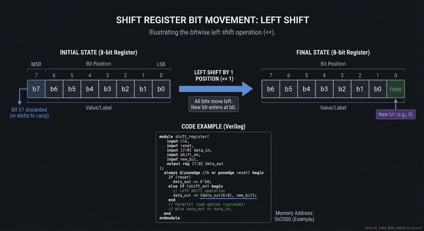
How It Works (Step-by-Step)
- Load a register with a value.
- On each clock edge, shift left or right.
- Insert a new bit at the shifted end.
Minimal Concrete Example
shift <= {shift[6:0], serial_in};
Common Misconceptions
- “Shift registers are only for serial I/O.” -> They are also for patterns and delays.
- “Shifts are free.” -> They still consume registers and routing.
Check-Your-Understanding Questions
- What is the difference between shift and rotate?
- How many cycles to shift out 8 bits?
- Why use shift registers in UART TX?
Where You’ll Apply It
- This project: used in Section 3.2 and Section 4
- Also used in: P15-uart-transmitter.md, P17-spi-master.md
Counters and Clock Enables
Description/Expanded Explanation of the concept
Counters are registers that increment or decrement each clock cycle. Clock enables allow you to update a register only when needed, which is safer than gating clocks. They are essential for timing, PWM, and pacing visible outputs.
Definitions & Key Terms
- Counter -> register that increments/decrements
- Clock enable -> condition that allows a register update
- Prescaler -> counter used to slow down a signal
Mental Model Diagram (ASCII)
clk -> [counter] --tick--> [slow logic]
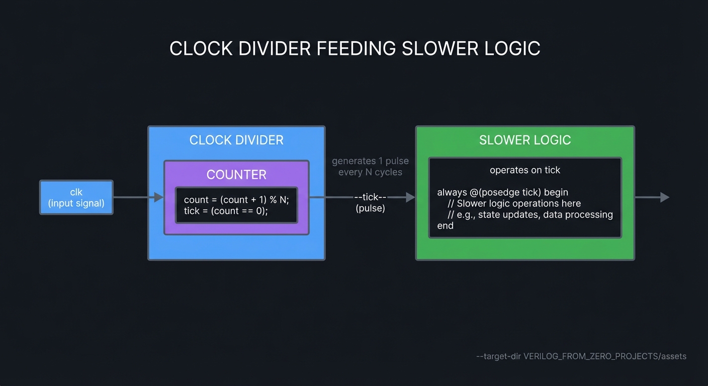
How It Works (Step-by-Step)
- Increment counter each clock edge.
- When counter reaches a limit, assert a tick.
- Use tick as a clock enable for slower logic.
Minimal Concrete Example
if (tick) out <= out + 1;
Common Misconceptions
- “Gating the clock is simpler.” -> It can break timing and glitch.
- “Counters are always free.” -> Wide counters consume resources.
Check-Your-Understanding Questions
- Why use clock enables instead of gating clocks?
- How do you choose counter width for a target frequency?
- What happens when a counter overflows?
Where You’ll Apply It
- This project: used in Section 3.2 and Section 5
- Also used in: P08-shift-register-led-chaser.md, P10-pwm-generator-led-dimmer-servo-control.md
Verification with Testbenches and Waveforms
Description/Expanded Explanation of the concept
Testbenches are simulation-only modules that apply stimulus and check outputs. Waveforms (VCD) are the hardware engineer’s microscope; they reveal timing, glitches, and ordering problems. A good testbench is deterministic and covers edge cases.
Definitions & Key Terms
- Testbench -> a non-synthesizable module that drives a DUT
- VCD -> Value Change Dump waveform file
- Deterministic test -> same inputs produce same outputs every run
Mental Model Diagram (ASCII)
[Testbench] -> [DUT] -> [VCD] -> [GTKWave]
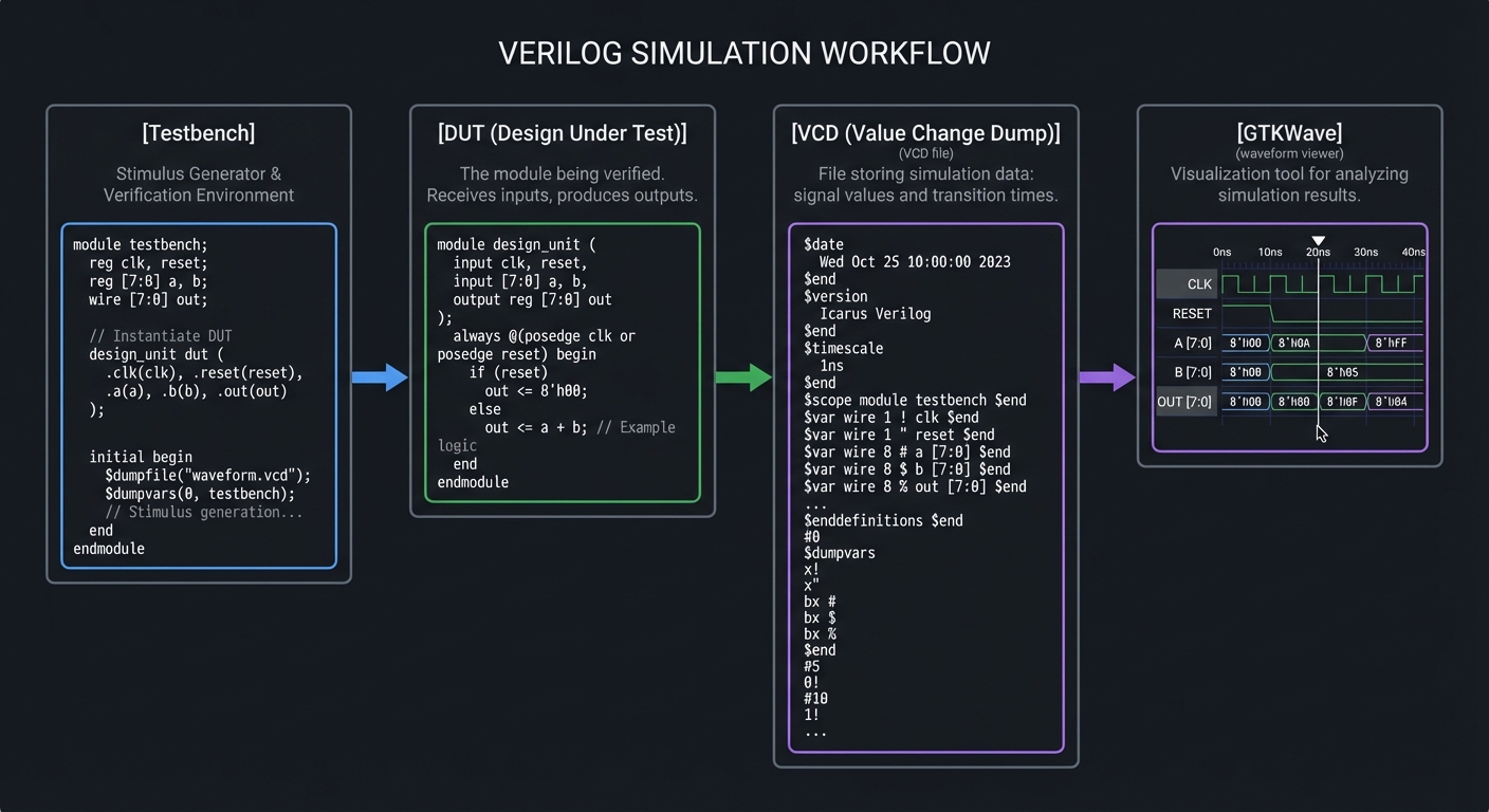
How It Works (Step-by-Step)
- Initialize inputs to known values.
- Apply stimulus over time.
- Dump waveforms and check outputs.
- Add assertions or PASS/FAIL messages.
Minimal Concrete Example
initial begin
  $dumpfile("wave.vcd");
  $dumpvars(0, tb);
  a = 0; b = 1; #10;
  $finish;
end
Common Misconceptions
- “If it simulates once, it’s correct.” -> Cover all relevant cases.
- “Waveforms are optional.” -> They are often the only way to debug timing.
Check-Your-Understanding Questions
- Why keep testbench and DUT separate?
- What is the purpose of
$dumpvars? - How do you make a testbench deterministic?
Where You’ll Apply It
- This project: used throughout Section 6 (testing)
- Also used in: all other projects in this folder
3. Project Specification
3.1 What You Will Build
An 8-bit shift register driving LEDs with a human-visible tick.
3.2 Functional Requirements
- Requirement 1: Shift left or right each tick
- Requirement 2: Reset to a known pattern
- Requirement 3: Optional bounce behavior at edges
3.3 Non-Functional Requirements
- Performance: Stable operation at the target clock and interfaces.
- Reliability: Deterministic outputs on all defined inputs.
- Usability: Clear ports and documented behavior.
3.4 Example Usage / Output
{p['example_usage']}
3.5 Data Formats / Schemas / Protocols
{p[‘data_format’]}
3.6 Edge Cases
- All zeros state
- Direction change
3.7 Real World Outcome
3.7.1 How to Run (Copy/Paste)
vvp shift_tb
3.7.2 Golden Path Demo (Deterministic)
Run the demo command above with the provided testbench and confirm the outputs match the golden transcript.
3.7.3 CLI Transcript
00000001
00000010
00000100
3.7.4 Failure Demo (Expected)
# Example failure case
ERROR: Output mismatch at vector 3
Expected: 0x0A, Got: 0x0B
EXIT CODE: 1
Notes:
- Exit code 0 indicates all tests passed
- Exit code 1 indicates a test failure
4. Solution Architecture
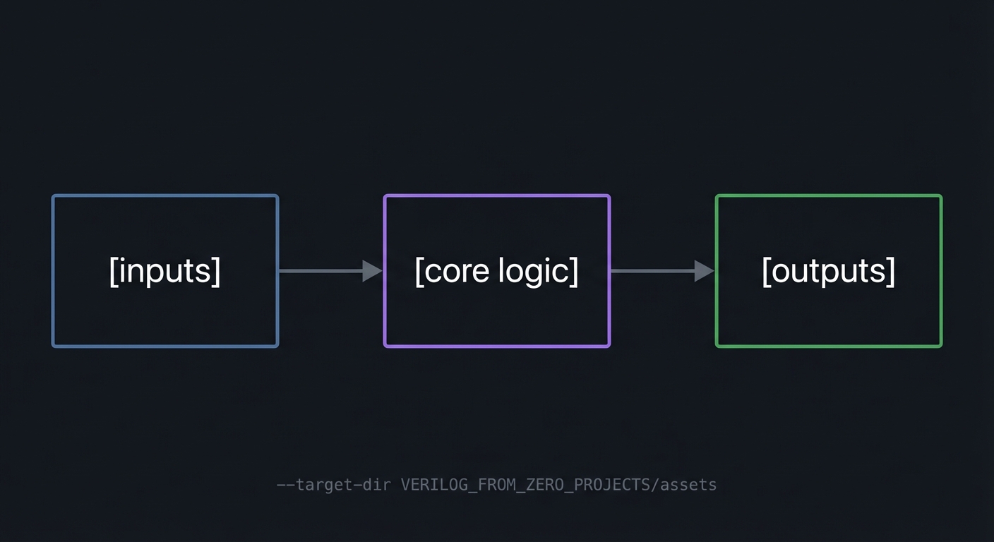
4.1 High-Level Design
[inputs] -> [core logic] -> [outputs]
4.2 Key Components
| Component | Responsibility |
|---|---|
| shifter | Shift register logic |
| prescaler | Slow tick generator |
4.3 Data Structures (No Full Code)
// Example signals (adapt to your design)
reg [7:0] state_reg;
reg [7:0] data_reg;
4.4 Algorithm Overview
Key Algorithm: Core control flow
- Initialize state/reset conditions.
- Apply inputs and compute outputs.
- Update state on clock edges (if sequential).
Complexity Analysis:
- Time: O(1) per cycle
- Space: O(N) for registers and logic
5. Implementation Guide
5.1 Development Environment Setup
iverilog -v
# Ensure GTKWave is installed for waveform viewing
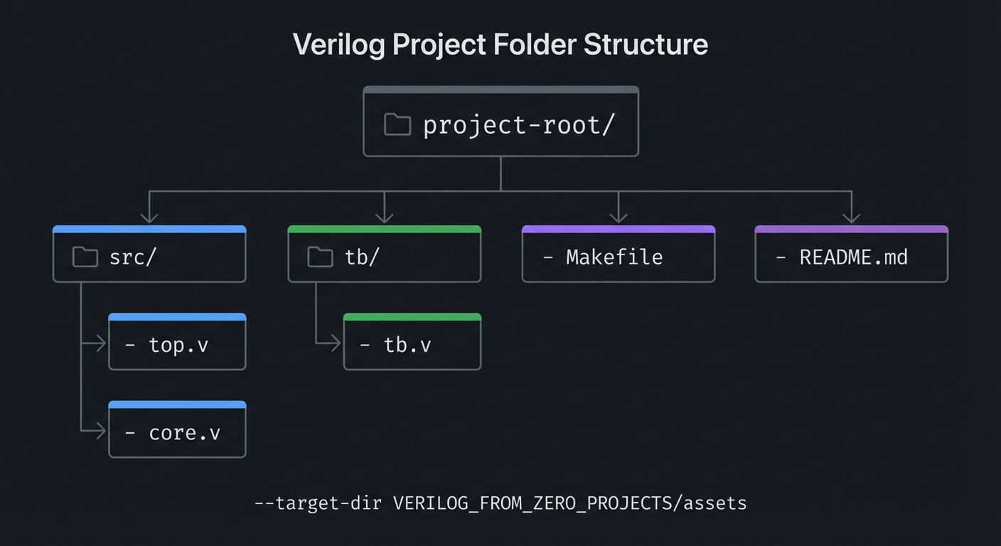
5.2 Project Structure
project-root/
|-- src/
|   |-- top.v
|   |-- core.v
|-- tb/
|   |-- tb.v
|-- Makefile
|-- README.md
5.3 The Core Question You’re Answering
“How do you create visible motion from a fast clock?”
5.4 Concepts You Must Understand First
- Shift registers
- Counters
5.5 Questions to Guide Your Design
- What tick rate is comfortable for human eyes?
- Do you want wrap or bounce?
5.6 Thinking Exercise
List the first 10 patterns for a bouncing LED.
5.7 The Interview Questions They’ll Ask
- What is a shift register?
- Why use clock enable instead of gating?
5.8 Hints in Layers
- Use a counter to generate a slow tick.
- Rotate bits to keep one LED on.
5.9 Books That Will Help
| Topic | Book | Chapter |
|---|---|---|
| Shift registers | Digital Design and Computer Architecture | Ch. 3 |
5.10 Implementation Phases
Phase 1: Foundation
Goals:
- Establish core module structure
- Implement minimal behavior
Tasks:
- Scaffold module ports and internal signals
- Write a minimal testbench that compiles
Checkpoint: Simulation runs without errors
Phase 2: Core Functionality
Goals:
- Implement full logic
- Verify edge cases
Tasks:
- Complete core logic
- Add directed tests for edge cases
Checkpoint: All tests pass and waveforms match expectations
Phase 3: Polish & Edge Cases
Goals:
- Improve readability
- Document behavior
Tasks:
- Add comments and README notes
- Expand tests for unusual inputs
Checkpoint: Design is deterministic and documented
5.11 Key Implementation Decisions
| Decision | Options | Recommendation | Rationale |
|---|---|---|---|
| Reset strategy | Sync / Async | Sync | Simpler timing closure |
| Test coverage | Directed / Exhaustive | Exhaustive for small logic | Prevents missed cases |
6. Testing Strategy
6.1 Test Categories
| Category | Purpose | Examples |
|---|---|---|
| Unit Tests | Test core logic | Small vectors |
| Integration Tests | Test modules together | Full system |
| Edge Case Tests | Boundary conditions | Max/min values |
6.2 Critical Test Cases
- Test 1: Pattern advances at each tick
- Test 2: Reset returns to initial pattern
6.3 Test Data
Use deterministic vectors and document expected outputs.
7. Common Pitfalls & Debugging
7.1 Frequent Mistakes
| Pitfall | Symptom | Solution |
|---|---|---|
| Too fast | LEDs blur | Increase prescaler |
7.2 Debugging Strategies
- Inspect waveforms at key internal signals
- Add temporary debug outputs to verify state
- Reduce testcases to the smallest failing case
7.3 Performance Traps
- Overly wide counters or combinational paths can reduce max clock
8. Extensions & Challenges
8.1 Beginner Extensions
- Add parameterization for widths
- Add optional features (enable, reset)
8.2 Intermediate Extensions
- Add configuration registers
- Build a simple driver or demo program
8.3 Advanced Extensions
- Integrate with another project in this series
- Implement a hardware demo on FPGA
9. Real-World Connections
9.1 Industry Applications
- Digital control systems and embedded peripherals
- FPGA prototyping and validation
9.2 Related Open Source Projects
- Yosys / nextpnr toolchain for open-source FPGA flow
- Example HDL projects in the FPGA community
9.3 Interview Relevance
- Demonstrates RTL thinking and verification skills
10. Resources
10.1 Essential Reading
- Digital Design and Computer Architecture - Focus on Ch. 3
10.2 Video Resources
- Search for project-specific HDL walkthroughs and waveforms
10.3 Tools & Documentation
- Icarus Verilog
- GTKWave
10.4 Related Projects in This Series
- See adjacent projects in
VERILOG_FROM_ZERO_PROJECTS/
11. Self-Assessment Checklist
11.1 Understanding
- I can explain the core concept without notes
- I can predict waveform behavior for basic inputs
11.2 Implementation
- All functional requirements are met
- All tests pass
- Edge cases are documented
11.3 Growth
- I can explain this project in an interview
- I documented at least one lesson learned
12. Submission / Completion Criteria
Minimum Viable Completion:
- Functional requirements implemented
- Testbench passes
- Waveforms inspected
Full Completion:
- All minimum criteria plus
- Edge cases covered and documented
Excellence (Going Above & Beyond):
- Hardware demo on FPGA
- Clear write-up of lessons learned
Appendix A: Deep Dive Walkthrough
A.1 Signal Map and Invariants
- Inputs:
clk,reset,en,seed[7:0](optional) - Outputs:
led[7:0]
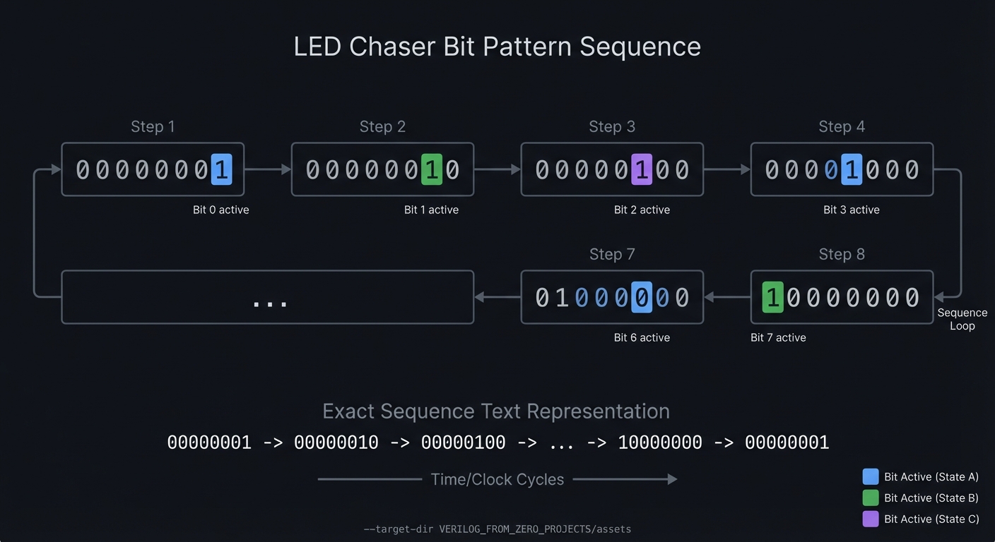
Invariant: Exactly one LED is on (one-hot) if using a ring counter.
A.2 Ring Counter Behavior
- Start with
00000001. - Each tick: shift left, wrap MSB to LSB.
00000001 -> 00000010 -> 00000100 -> ... -> 10000000 -> 00000001
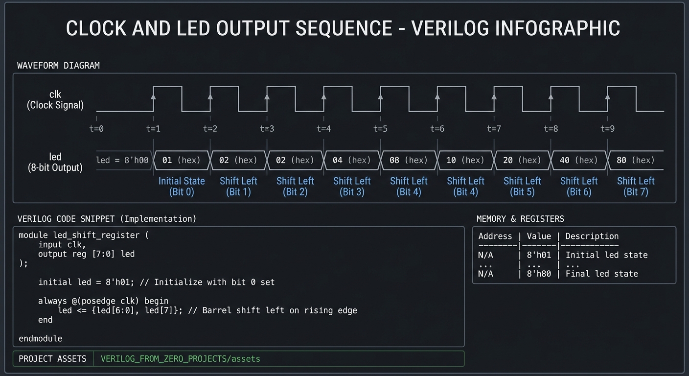
A.3 Timing Sketch
clk: _/\_/\_/\_/\_
led: 01 02 04 08 10 20 40 80 (hex)
A.4 Deterministic Test Sequence
- Apply reset -> expect
led=1. - Enable for 8 cycles -> expect return to
1. - Disable
enand verify hold.
A.5 Extension Notes
- Add direction control for reverse chase.
- Add PWM dimming per LED for brightness effects.
13. Deep Dive Appendix
13.1 Timing and Resource Budget
- Shift registers are just registers with bit movement each clock.
- The only timing cost is the clock-to-Q plus the shift mux.
- The speed of the LED chaser is set by your clock divider.
13.2 Waveform Interpretation Guide
- shift_reg should move the single 1 bit each tick.
- If you implement rotation, the MSB should wrap to LSB cleanly.
Example:
0001 -> 0010 -> 0100 -> 1000 -> 0001
13.3 Hardware Bring-Up Notes
- Drive 4 or 8 LEDs directly from shift register bits.
- Use a slow divider (1-10 Hz) to see the motion.
- If your board has a reset button, use it to re-center the chaser.
13.4 Alternate Implementations and Trade-offs
- Shift with zero fill: pattern disappears over time.
- Rotate: ring counter style; pattern repeats.
- LFSR: pseudo-random pattern for a more interesting chase.
13.5 Additional Exercises
- Add direction control and reverse the chase with a switch.
- Add speed control using a small counter for multiple speeds.
- Create two independent chasers and XOR their patterns.