Project 3: 7-Segment Display Decoder
Map hex digits 0-F into 7-seg LED patterns and verify with simulation.
Quick Reference
| Attribute | Value |
|---|---|
| Difficulty | Beginner |
| Time Estimate | 3-4 hours |
| Main Programming Language | Verilog (Alternatives: VHDL, SystemVerilog) |
| Alternative Programming Languages | VHDL, SystemVerilog |
| Coolness Level | Medium |
| Business Potential | Low |
| Prerequisites | Truth tables, Combinational logic |
| Key Topics | Encoding, Segment mapping, Active-low signals |
1. Learning Objectives
- Build a decoder lookup table
- Document segment polarity and wiring
- Write a testbench for all 16 hex values
2. All Theory Needed (Per-Concept Breakdown)
Boolean Algebra and Truth Tables
Description/Expanded Explanation of the concept
Boolean algebra is the math of digital logic. A truth table is the exact, exhaustive mapping from inputs to outputs. In hardware, there is no “default” or “implicit” behavior: every input combination must map to a defined output. This is the foundation of reliable combinational circuits.
Definitions & Key Terms
- Boolean algebra -> algebra of 0/1 variables with AND/OR/NOT operators
- Truth table -> exhaustive input/output mapping
- Minterm -> AND of variables producing 1 for one input combination
- Maxterm -> OR of variables producing 0 for one input combination
Mental Model Diagram (ASCII)
Inputs -> [Truth Table] -> Boolean Expression -> Gates
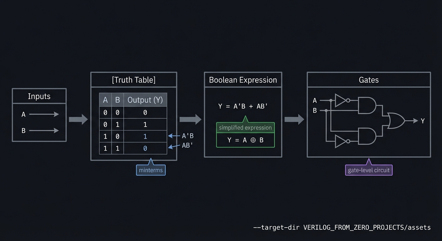
How It Works (Step-by-Step)
- List all input combinations.
- Mark which combinations should produce 1.
- Translate the table into an expression or directly into gates.
- Verify with exhaustive simulation.
Minimal Concrete Example
// AND gate truth table: y = a & b
assign y = a & b;
Common Misconceptions
- “If it works for some cases, it’s fine.” -> All cases must be correct.
- “Truth tables are only for beginners.” -> They remain the most reliable spec.
Check-Your-Understanding Questions
- What output should an XOR produce for inputs 01 and 10?
- How many rows does a truth table have for 4 inputs?
- Explain why a missing row is a bug in hardware.
Where You’ll Apply It
- This project: used in Section 3.2 (functional requirements) and Section 6 (testing)
- Also used in: P02-4-to-1-multiplexer.md, P03-7-segment-display-decoder.md
Combinational Logic Modeling
Description/Expanded Explanation of the concept
Combinational logic produces outputs that depend only on current inputs. In Verilog, this is modeled using assign or always @(*) blocks. The key rule is that every output must be assigned for every input condition, otherwise you create unintended storage (latches).
Definitions & Key Terms
- Combinational logic -> outputs depend only on current inputs
- Continuous assignment ->
assignfor wire-driven logic - Latch -> unintended storage inferred by incomplete assignments
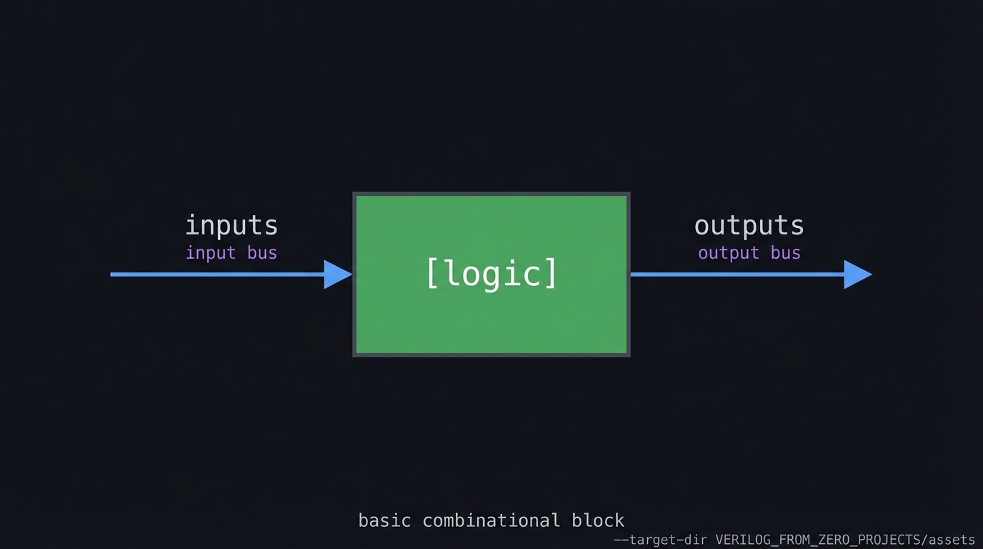
Mental Model Diagram (ASCII)
inputs --> [logic] --> outputs
How It Works (Step-by-Step)
- Choose
assignfor simple logic oralways @(*)for complex logic. - Ensure outputs are assigned in all branches.
- Verify with exhaustive or directed tests.
Minimal Concrete Example
always @(*) begin
  if (sel) y = b; else y = a;
end
Common Misconceptions
- “Missing default just means don’t care.” -> It creates a latch.
- “Blocking assignments are always wrong.” -> They are correct in combinational blocks.
Check-Your-Understanding Questions
- What hardware does an if/else create?
- Why does a missing default create storage?
- When should you use
assignvsalways @(*)?
Where You’ll Apply It
- This project: used in Section 3.2 and Section 5.3
- Also used in: P01-digital-gate-library.md, P03-7-segment-display-decoder.md, P04-4-bit-ripple-carry-adder.md
Verification with Testbenches and Waveforms
Description/Expanded Explanation of the concept
Testbenches are simulation-only modules that apply stimulus and check outputs. Waveforms (VCD) are the hardware engineer’s microscope; they reveal timing, glitches, and ordering problems. A good testbench is deterministic and covers edge cases.
Definitions & Key Terms
- Testbench -> a non-synthesizable module that drives a DUT
- VCD -> Value Change Dump waveform file
- Deterministic test -> same inputs produce same outputs every run
Mental Model Diagram (ASCII)
[Testbench] -> [DUT] -> [VCD] -> [GTKWave]
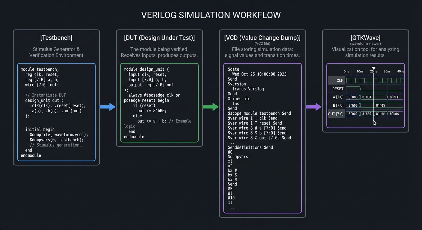
How It Works (Step-by-Step)
- Initialize inputs to known values.
- Apply stimulus over time.
- Dump waveforms and check outputs.
- Add assertions or PASS/FAIL messages.
Minimal Concrete Example
initial begin
  $dumpfile("wave.vcd");
  $dumpvars(0, tb);
  a = 0; b = 1; #10;
  $finish;
end
Common Misconceptions
- “If it simulates once, it’s correct.” -> Cover all relevant cases.
- “Waveforms are optional.” -> They are often the only way to debug timing.
Check-Your-Understanding Questions
- Why keep testbench and DUT separate?
- What is the purpose of
$dumpvars? - How do you make a testbench deterministic?
Where You’ll Apply It
- This project: used throughout Section 6 (testing)
- Also used in: all other projects in this folder
3. Project Specification
3.1 What You Will Build
A combinational decoder that maps 4-bit hex inputs to a 7-bit segment pattern.
3.2 Functional Requirements
- Requirement 1: Support hex inputs 0-F
- Requirement 2: Define segment polarity (active-high or active-low)
- Requirement 3: Provide a testbench that loops through 0-15
3.3 Non-Functional Requirements
- Performance: Stable operation at the target clock and interfaces.
- Reliability: Deterministic outputs on all defined inputs.
- Usability: Clear ports and documented behavior.
3.4 Example Usage / Output
{p['example_usage']}
3.5 Data Formats / Schemas / Protocols
{p[‘data_format’]}
3.6 Edge Cases
- Undefined input > 0xF
- Segment polarity mismatches
3.7 Real World Outcome
3.7.1 How to Run (Copy/Paste)
vvp seg7_tb
3.7.2 Golden Path Demo (Deterministic)
Run the demo command above with the provided testbench and confirm the outputs match the golden transcript.
3.7.3 CLI Transcript
0 -> 0b0111111
1 -> 0b0000110
A -> 0b1110111
F -> 0b1110001
3.7.4 Failure Demo (Expected)
# Example failure case
ERROR: Output mismatch at vector 3
Expected: 0x0A, Got: 0x0B
EXIT CODE: 1
Notes:
- Exit code 0 indicates all tests passed
- Exit code 1 indicates a test failure
4. Solution Architecture
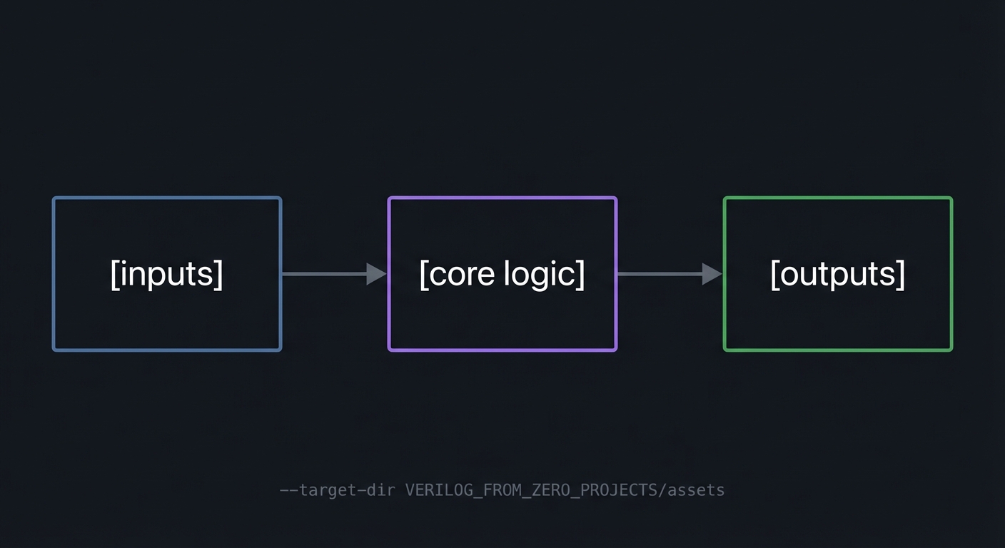
4.1 High-Level Design
[inputs] -> [core logic] -> [outputs]
4.2 Key Components
| Component | Responsibility |
|---|---|
| seg7 | Decoder logic |
| seg7_tb | Testbench with 0-F sweep |
4.3 Data Structures (No Full Code)
// Example signals (adapt to your design)
reg [7:0] state_reg;
reg [7:0] data_reg;
4.4 Algorithm Overview
Key Algorithm: Core control flow
- Initialize state/reset conditions.
- Apply inputs and compute outputs.
- Update state on clock edges (if sequential).
Complexity Analysis:
- Time: O(1) per cycle
- Space: O(N) for registers and logic
5. Implementation Guide
5.1 Development Environment Setup
iverilog -v
# Ensure GTKWave is installed for waveform viewing
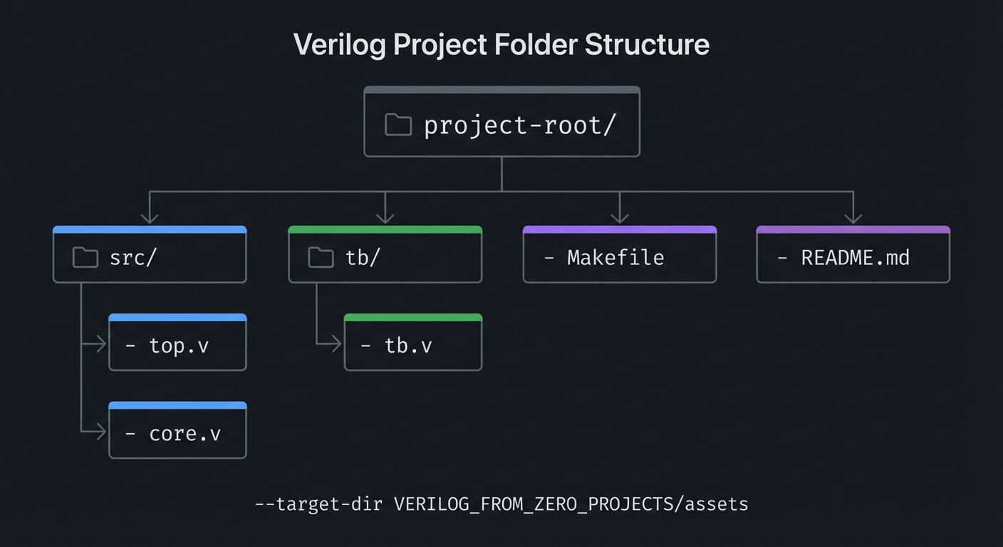
5.2 Project Structure
project-root/
|-- src/
|   |-- top.v
|   |-- core.v
|-- tb/
|   |-- tb.v
|-- Makefile
|-- README.md
5.3 The Core Question You’re Answering
“How do you map symbolic values to physical LED segments?”
5.4 Concepts You Must Understand First
- Truth tables
- Combinational logic
5.5 Questions to Guide Your Design
- Are your segments active-high or active-low?
- Will you support hex or only decimal?
5.6 Thinking Exercise
Draw a 7-seg display and list which segments light for ‘A’ and ‘F’.
5.7 The Interview Questions They’ll Ask
- Why do some displays use active-low signals?
- What is multiplexing and why is it needed?
- How do you avoid magic numbers in a decoder?
5.8 Hints in Layers
- Start with a case statement mapping each nibble.
- Use named parameters for segments.
5.9 Books That Will Help
| Topic | Book | Chapter |
|---|---|---|
| Encoding and logic | Digital Design and Computer Architecture | Ch. 2 |
| Verilog case tables | Digital Design and Computer Architecture | Ch. 4 |
5.10 Implementation Phases
Phase 1: Foundation
Goals:
- Establish core module structure
- Implement minimal behavior
Tasks:
- Scaffold module ports and internal signals
- Write a minimal testbench that compiles
Checkpoint: Simulation runs without errors
Phase 2: Core Functionality
Goals:
- Implement full logic
- Verify edge cases
Tasks:
- Complete core logic
- Add directed tests for edge cases
Checkpoint: All tests pass and waveforms match expectations
Phase 3: Polish & Edge Cases
Goals:
- Improve readability
- Document behavior
Tasks:
- Add comments and README notes
- Expand tests for unusual inputs
Checkpoint: Design is deterministic and documented
5.11 Key Implementation Decisions
| Decision | Options | Recommendation | Rationale |
|---|---|---|---|
| Reset strategy | Sync / Async | Sync | Simpler timing closure |
| Test coverage | Directed / Exhaustive | Exhaustive for small logic | Prevents missed cases |
6. Testing Strategy
6.1 Test Categories
| Category | Purpose | Examples |
|---|---|---|
| Unit Tests | Test core logic | Small vectors |
| Integration Tests | Test modules together | Full system |
| Edge Case Tests | Boundary conditions | Max/min values |
6.2 Critical Test Cases
- Test 1: Sweep 0-15 and compare against table
- Test 2: Confirm no X/Z in output
6.3 Test Data
Use deterministic vectors and document expected outputs.
7. Common Pitfalls & Debugging
7.1 Frequent Mistakes
| Pitfall | Symptom | Solution |
|---|---|---|
| Wrong segment order | Digits are scrambled | Re-map bit order to match wiring |
7.2 Debugging Strategies
- Inspect waveforms at key internal signals
- Add temporary debug outputs to verify state
- Reduce testcases to the smallest failing case
7.3 Performance Traps
- Overly wide counters or combinational paths can reduce max clock
8. Extensions & Challenges
8.1 Beginner Extensions
- Add parameterization for widths
- Add optional features (enable, reset)
8.2 Intermediate Extensions
- Add configuration registers
- Build a simple driver or demo program
8.3 Advanced Extensions
- Integrate with another project in this series
- Implement a hardware demo on FPGA
9. Real-World Connections
9.1 Industry Applications
- Digital control systems and embedded peripherals
- FPGA prototyping and validation
9.2 Related Open Source Projects
- Yosys / nextpnr toolchain for open-source FPGA flow
- Example HDL projects in the FPGA community
9.3 Interview Relevance
- Demonstrates RTL thinking and verification skills
10. Resources
10.1 Essential Reading
- Digital Design and Computer Architecture - Focus on Ch. 2
- Digital Design and Computer Architecture - Focus on Ch. 4
10.2 Video Resources
- Search for project-specific HDL walkthroughs and waveforms
10.3 Tools & Documentation
- Icarus Verilog
- GTKWave
10.4 Related Projects in This Series
- See adjacent projects in
VERILOG_FROM_ZERO_PROJECTS/
11. Self-Assessment Checklist
11.1 Understanding
- I can explain the core concept without notes
- I can predict waveform behavior for basic inputs
11.2 Implementation
- All functional requirements are met
- All tests pass
- Edge cases are documented
11.3 Growth
- I can explain this project in an interview
- I documented at least one lesson learned
12. Submission / Completion Criteria
Minimum Viable Completion:
- Functional requirements implemented
- Testbench passes
- Waveforms inspected
Full Completion:
- All minimum criteria plus
- Edge cases covered and documented
Excellence (Going Above & Beyond):
- Hardware demo on FPGA
- Clear write-up of lessons learned
Appendix A: Deep Dive Walkthrough
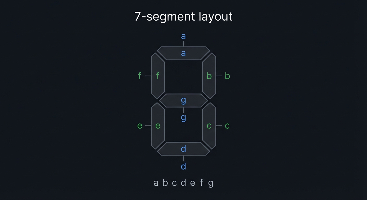
A.1 Signal Map and Invariants
- Input:
hex[3:0] - Outputs:
seg[6:0]in order{a,b,c,d,e,f,g} - Assumption: Common-cathode (1 = segment ON). Adjust if common-anode.
Invariant: For digits 0-9 (and A-F if you support hex), segments match the canonical glyphs.
A.2 Reference Glyph Table (Common-Cathode)
| Hex | Segments On (a b c d e f g) | seg[6:0] | |—–|—————————–|———-| | 0 | a b c d e f | 1111110 | | 1 | b c | 0110000 | | 2 | a b d e g | 1101101 | | 3 | a b c d g | 1111001 | | 4 | b c f g | 0110011 | | 5 | a c d f g | 1011011 | | 6 | a c d e f g | 1011111 | | 7 | a b c | 1110000 | | 8 | a b c d e f g | 1111111 | | 9 | a b c d f g | 1111011 |
A.3 ASCII Segment Map
  a
 f b
  g
 e c
  d
A.4 Deterministic Testbench Pattern
- Step
hexfrom 0 to 9. - Capture
segand compare against the table above. - For hex A-F (optional), add a second table and validate.
A.5 Hardware Wiring Notes
- Common-anode displays require inverted outputs.
- Segment order in your board constraints may not match
{a,b,c,d,e,f,g}. Use a wiring map and document it in the testbench.
13. Deep Dive Appendix
13.1 Timing and Resource Budget
- Decoder logic is purely combinational; it maps to LUTs with minimal depth.
- If you target a multiplexed display later, you will add a scan clock, but the decoder itself stays combinational.
- Consider active-high vs active-low segments early so you do not invert twice.
13.2 Waveform Interpretation Guide
- For each input nibble, inspect seg[6:0] and confirm the correct segments light.
- Watch for polarity: common-anode displays require inverted outputs.
Example mapping (common-cathode, segments a-g):
0 -> 0b0111111
1 -> 0b0000110
2 -> 0b1011011
13.3 Hardware Bring-Up Notes
- Use current-limiting resistors for each segment.
- Confirm whether your module is common-anode or common-cathode.
- Drive only one digit at a time if you do not implement multiplexing.
13.4 Alternate Implementations and Trade-offs
- Case/lookup table: simplest and clearest.
- ROM-based: store patterns in a small memory array.
- Logic minimization: minimize the Boolean equations for fewer LUTs (good exercise).
13.5 Additional Exercises
- Expand to hex digits (A-F) with distinct segment patterns.
- Add a decimal point control bit.
- Combine with a multiplexer to support multiple digits.