CPU, ISA & Computer Architecture - Learning Projects
Goal: Build a first-principles understanding of how real CPUs execute instructions, move data, and coordinate the whole system. By completing these projects you will internalize the ISA vs microarchitecture split, learn how instructions are encoded and decoded, reason about register files and control flow, and understand why memory hierarchy, caches, and pipelines dominate performance. You will be able to read assembly and machine code with confidence, design a small ISA, emulate historical CPUs, and explain how modern processors turn programs into electrical signals and back into results.
Why CPU, ISA, and Architecture Matter
Every software system is ultimately executed as machine instructions on a real CPU. The ISA is the contract, the microarchitecture is the implementation, and everything above it depends on these details.
- Debugging: crashes and performance regressions often come down to instruction ordering, cache misses, or branch behavior.
- Security: most low-level vulnerabilities are instruction- and memory-precise (buffer overflows, speculative leaks, code-reuse).
- Performance: “fast code” is code that matches the CPU’s execution and memory model, not just the language model.
The mental model you are building in this file is the same one used by compiler authors, emulator writers, and CPU designers.
Source Code -> Compiler -> ISA Instructions -> Microarchitecture -> Gates -> Electrons
     ^                         |                    |
     |                         |                    +-- pipelines, caches, branch prediction
     |                         +-- opcodes, registers, addressing modes
     +-- what you write
Prerequisites & Background Knowledge
Essential Prerequisites (Must Have)
- Comfortable with C or another systems language
- Basic data structures (arrays, stacks)
- Familiarity with binary and hex notation
Helpful But Not Required
- Basic assembly exposure
- Digital logic fundamentals (AND/OR/XOR, flip-flops)
- Debugger experience (gdb/lldb)
Self-Assessment Questions
- Can you explain why
0xFFequals 255? - Do you know the difference between a register and memory?
- Have you ever read a hex dump and recognized text or numbers?
Development Environment Setup
- C compiler (GCC or Clang)
- A hex editor or
xxdfor inspection - Optional:
nasm/asfor assembly experiments
Time Investment
- Foundation projects: 2-4 weeks total
- Emulators and ISA design: 4-8 weeks
- Hardware pipeline/FPGA work: 2-4 months
Important Reality Check
These projects are intentionally low-level. Expect to spend time reading specs and stepping through instructions. This is the point.
Core Concept Analysis
1) ISA vs Microarchitecture
The ISA is the programmer-visible contract: registers, instructions, addressing modes. The microarchitecture is how the CPU actually implements the contract.
ISA Contract:     "ADD R1, R2, R3 means R1 = R2 + R3"
Microarchitecture: Fetch -> Decode -> Execute -> Writeback (with pipelines, caches, predictors)
2) Instruction Encoding and Addressing
Every instruction is a binary pattern with fields for opcode and operands.
32-bit Instruction (example)
┌──────────┬─────┬─────┬─────┬──────────┐
│ opcode   │ rs1 │ rs2 │ rd  │ immediate│
└──────────┴─────┴─────┴─────┴──────────┘
Addressing modes decide how operands are found: immediate, register, memory, indirect, indexed.
3) Registers, ALU, and Status Flags
Registers are the CPU’s fastest storage. The ALU performs arithmetic and logic, and status flags record conditions (zero, negative, carry, overflow).
R1 + R2 -> ALU -> R3
         |         |
         +----> flags (Z, N, C, V)
4) Fetch-Decode-Execute and Control Flow
The CPU repeatedly fetches instructions, decodes them, and executes them. Control flow (branches, calls, returns) changes the program counter.
PC -> Fetch -> Decode -> Execute -> Update PC -> repeat
5) Memory Hierarchy and Caches
CPU speed is limited by memory latency. Caches exist to keep hot data near the CPU.
Registers -> L1 Cache -> L2 Cache -> L3 Cache -> RAM -> Disk
  1 cycle     ~4 cycles   ~10-20      ~30-50     100+   10k+
6) Exceptions, Interrupts, and I/O
Interrupts are how the CPU responds to external events. Exceptions handle faults (divide by zero, page faults).
Device -> Interrupt -> CPU saves state -> Handler -> Resume
7) Pipelining, Hazards, and Speculation
Modern CPUs overlap instructions. Hazards occur when dependencies or branches break the pipeline, and predictors guess to keep it full.
IF | ID | EX | MEM | WB
8) Emulation vs Simulation vs Hardware
- Emulation: interpret or translate one ISA on another.
- Simulation: model a CPU to study timing and design.
- Hardware: implement a real CPU in logic (FPGA/ASIC).
Concept Summary Table
| Concept Cluster | What You Need to Internalize |
|---|---|
| Data Representation | Binary/hex are the CPU’s native language; signed values are two’s complement. |
| Instruction Sets | ISAs define opcodes, operands, and addressing modes that software targets. |
| Datapath & Control | Registers, ALU, and control logic implement the fetch-decode-execute loop. |
| Control Flow | Branches, calls, and returns are PC rewrites with stack support. |
| Memory Hierarchy | Performance is dominated by cache locality and memory latency. |
| Exceptions & I/O | Interrupts and faults redirect execution to handlers. |
| Pipelining | Overlapped execution improves throughput but introduces hazards. |
| Emulation & Hardware | Understanding ranges from software models to real silicon. |
Deep Dive Reading By Concept
| Concept | Book & Chapter |
|---|---|
| ISA design and instruction encoding | Computer Organization and Design (RISC-V Edition) by Patterson & Hennessy - Ch. 2-4 |
| Fetch-decode-execute and datapath | Computer Organization and Design by Patterson & Hennessy - Ch. 4 |
| CPU performance and pipelining | Computer Architecture by Hennessy & Patterson - Ch. 3-4 |
| Data representation and two’s complement | Code: The Hidden Language by Charles Petzold - Ch. 7-10 |
| Cache organization and locality | Computer Systems: A Programmer’s Perspective by Bryant & O’Hallaron - Ch. 6 |
| Low-level execution and assembly | Inside the Machine by Jon Stokes - Ch. 1-4 |
| Digital logic and hardware design | Digital Design and Computer Architecture by Harris & Harris - Ch. 1-5 |
Quick Start (First 48 Hours)
- Build the Binary & Hex Visualizer to internalize numeric representation.
- Implement the Logic Gate Simulator and construct a 1-bit adder.
- Read a few pages of any ISA reference (RISC-V, 6502, or x86) to see real opcodes.
- Run a tiny program and trace it instruction-by-instruction in your debugger.
Recommended Learning Paths
Path A: The Software Systems Path (4-8 weeks)
- Binary/Hex Visualizer
- Logic Gate Simulator
- Stack Machine VM
- CHIP-8 Emulator
- Custom RISC CPU
- Cache or Pipeline Simulator
Path B: The Emulator Builder Path (6-10 weeks)
- Binary/Hex Visualizer
- Stack Machine VM
- CHIP-8 Emulator
- 6502 Emulator
- Game Boy Emulator
Path C: The Hardware Path (8-16+ weeks)
- Logic Gate Simulator
- Custom RISC CPU
- Pipeline Simulator
- RISC-V CPU on FPGA
Table of Contents
- Project 1: Binary & Hex Visualization Tool
- Project 2: Logic Gate Simulator
- Project 3: Stack Machine Virtual Machine
- Project 4: CHIP-8 Emulator
- Project 5: Simple RISC CPU Emulator (Custom ISA)
- Project 6: 6502 CPU Emulator (NES/C64 CPU)
- Project 7: Memory Visualizer & Debugger
- Project 8: x86-64 Disassembler
- Project 9: Write Programs in Assembly (x86-64 or ARM)
- Project 10: Game Boy Emulator (Z80-like CPU)
- Project 11: Bare-Metal Programming (Raspberry Pi or Arduino)
- Project 12: RISC-V CPU on FPGA
- Project 13: CPU Pipeline Simulator
- Project 14: Cache Simulator
- Project 15: Branch Predictor Simulator
- Capstone: RISC-V System-on-Chip with Peripherals
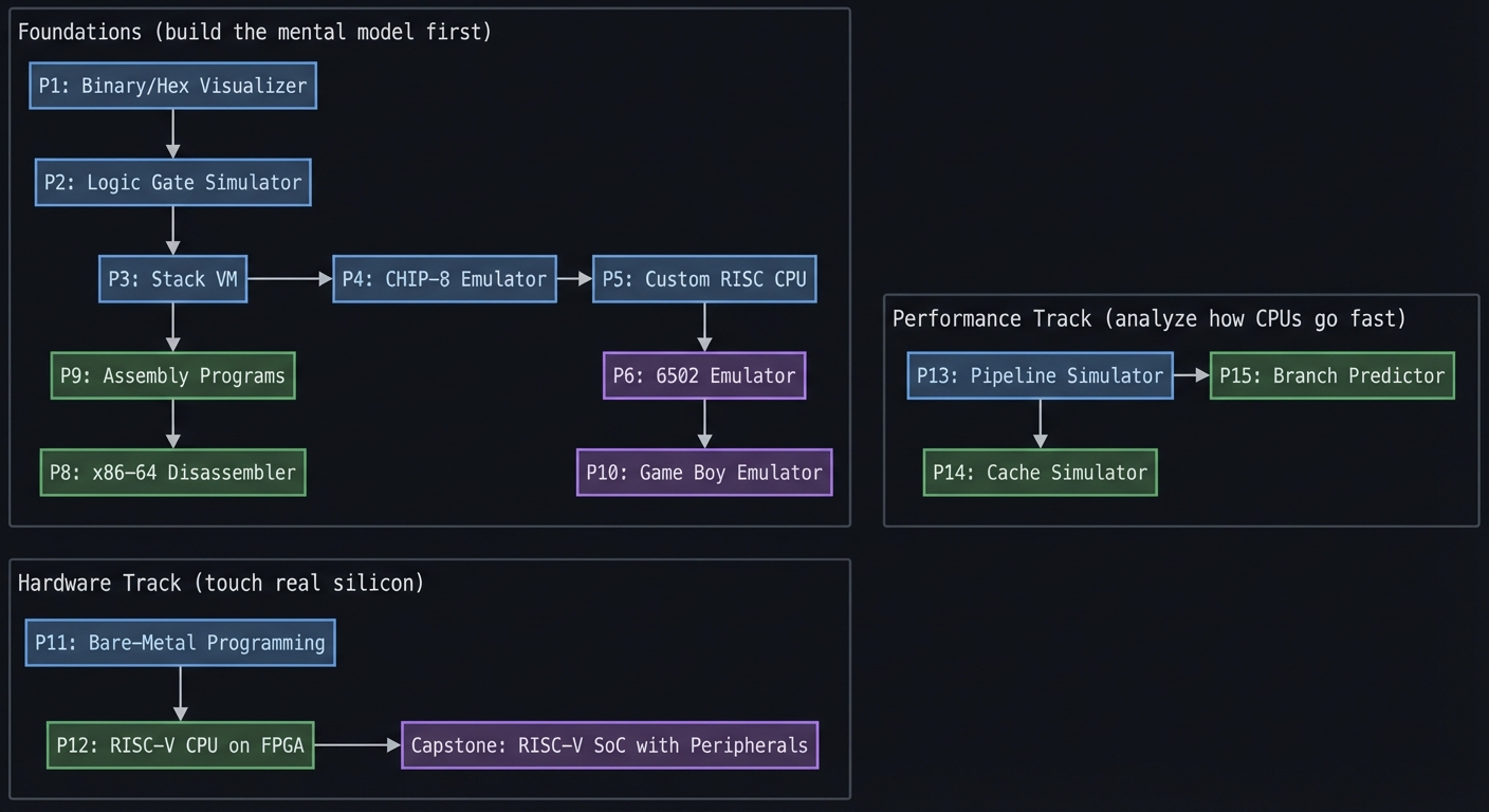
Project Dependency Graph
Foundations (build the mental model first)
  P1: Binary/Hex Visualizer
  P2: Logic Gate Simulator
           |
           v
  P3: Stack VM -----> P4: CHIP-8 Emulator -----> P5: Custom RISC CPU
           |                                      |
           v                                      v
  P9: Assembly Programs                     P6: 6502 Emulator
           |                                      |
           v                                      v
  P8: x86-64 Disassembler                  P10: Game Boy Emulator

Performance Track (analyze how CPUs go fast)
  P13: Pipeline Simulator -----> P15: Branch Predictor
                 |
                 v
          P14: Cache Simulator

Hardware Track (touch real silicon)
  P11: Bare-Metal Programming
           |
           v
  P12: RISC-V CPU on FPGA -----> Capstone: RISC-V SoC with Peripherals
Project 1: Binary & Hex Visualization Tool
- File: CPU_ISA_ARCHITECTURE_PROJECTS.md
- Main Programming Language: C
- Alternative Programming Languages: Python, Rust, Go
- Coolness Level: Level 2: Practical but Forgettable
- Business Potential: 1. The “Resume Gold” (Educational/Personal Brand)
- Difficulty: Level 1: Beginner (The Tinkerer)
- Knowledge Area: Number Systems / Data Representation
- Software or Tool: CLI Converter Tool
- Main Book: “Code: The Hidden Language of Computer Hardware and Software” by Charles Petzold
What you’ll build: A command-line tool that converts between decimal, binary, hexadecimal, and shows the actual bit patterns with visual highlighting of sign bits, byte boundaries, and two’s complement representation.
Why it teaches CPU fundamentals: CPUs don’t understand decimal—everything is binary. Before you can understand instructions, you must be fluent in reading hex dumps and binary patterns. This forces you to internalize how numbers are actually stored.
Core challenges you’ll face:
- Implementing two’s complement for negative numbers → maps to how CPUs represent signed integers
- Handling different bit widths (8, 16, 32, 64-bit) → maps to register sizes and data types
- Displaying byte order (little-endian vs big-endian) → maps to memory layout differences between architectures
- Parsing and validating input in multiple bases → maps to how assemblers parse numeric literals
Key Concepts:
- Binary Number System: “Code” Chapter 7-9 - Charles Petzold
- Two’s Complement: “Computer Systems: A Programmer’s Perspective” Chapter 2.2 - Bryant & O’Hallaron
- Endianness: “Computer Systems: A Programmer’s Perspective” Chapter 2.1.3 - Bryant & O’Hallaron
- Bit Manipulation in C: “The C Programming Language” Chapter 2.9 - Kernighan & Ritchie
Difficulty: Beginner Time estimate: Weekend Prerequisites: Basic C programming, understanding of decimal numbers
Real world outcome:
$ ./bitview 255
Decimal:     255
Binary:      00000000 00000000 00000000 11111111
Hex:         0x000000FF
Signed:      255 (positive)
Bit width:   32-bit

$ ./bitview -1
Decimal:     -1
Binary:      11111111 11111111 11111111 11111111
Hex:         0xFFFFFFFF
Signed:      -1 (two's complement)

$ ./bitview 0xDEADBEEF
Decimal:     3735928559
Binary:      11011110 10101101 10111110 11101111
             ^^^^^^^^ ^^^^^^^^ ^^^^^^^^ ^^^^^^^^
                DE       AD       BE       EF
The core question you’re answering: How do CPUs interpret the same bits as signed/unsigned values, and why does width and endianness change meaning?
Concepts you must understand first:
- Two’s complement and sign extension
- Word size vs data size (8/16/32/64-bit)
- Endianness and byte order
- Bitwise operators and masking
Questions to guide your design:
- How will you detect input base (0b, 0x, decimal)?
- How will you normalize values to a specific width?
- How will you visualize byte boundaries and sign bits?
Thinking exercise: Convert -13 to 8-bit two’s complement and explain why the top bit flips to 1. Now do the same in 16-bit and note the difference.
The interview questions they’ll ask:
- Why does two’s complement make subtraction easy for ALUs?
- What is the difference between signed and unsigned overflow?
- How do you detect endianness at runtime?
- Why is hex the standard for memory inspection?
Hints in layers:
- Hint 1: Use
strtoullwith base 0 to accept0xand decimal, then handle0bmanually. - Hint 2: Normalize to width with a mask:
value & ((1ULL << width) - 1). - Hint 3: Print bits by iterating from
width - 1to0and insert a space every 8 bits.
Books that will help:
| Topic | Book & Chapter |
|---|---|
| Two’s complement | Computer Systems: A Programmer’s Perspective - Ch. 2 |
| Binary and hex | Code: The Hidden Language - Ch. 7-9 |
| Bitwise operations | The C Programming Language - Ch. 2 |
Common pitfalls & debugging:
- Problem: Negative numbers print with unexpected hex values.
Why: You are not masking to the chosen width.
Fix: Apply a width mask before formatting.
Quick test:-1in 8-bit should show0xFF. - Problem: Endianness output looks reversed.
Why: You are printing bits, not bytes.
Fix: Group by bytes and reverse the byte order for big-endian view.
Learning milestones:
- Decimal-to-binary conversion works → You understand positional number systems
- Two’s complement displays correctly for negative numbers → You understand how CPUs handle signed arithmetic
- Endianness display toggle works → You understand memory layout fundamentals
Project 2: Logic Gate Simulator
- File: CPU_ISA_ARCHITECTURE_PROJECTS.md
- Main Programming Language: C
- Alternative Programming Languages: Rust, Python, JavaScript (for visual version)
- Coolness Level: Level 3: Genuinely Clever
- Business Potential: 1. The “Resume Gold” (Educational/Personal Brand)
- Difficulty: Level 1: Beginner (The Tinkerer)
- Knowledge Area: Digital Logic / Boolean Algebra
- Software or Tool: Logic Simulator
- Main Book: “Code: The Hidden Language of Computer Hardware and Software” by Charles Petzold
What you’ll build: A simulator where you can wire together AND, OR, NOT, XOR, NAND gates to build circuits. You’ll then build a 1-bit adder, then chain them into an 8-bit adder—the core of an ALU.
Why it teaches CPU fundamentals: CPUs are just billions of logic gates. By building an adder from gates, you see that “addition” isn’t magic—it’s just carefully arranged AND/OR/XOR gates. This demystifies the ALU completely.
Core challenges you’ll face:
- Implementing gate propagation (output depends on inputs) → maps to combinational logic
- Building a half-adder, then full-adder → maps to how ALUs perform arithmetic
- Chaining adders with carry propagation → maps to why addition takes time (carry delay)
- Detecting overflow → maps to CPU status flags
Key Concepts:
- Boolean Algebra: “Code” Chapter 10-11 - Charles Petzold
- Logic Gates: “Digital Design and Computer Architecture” Chapter 1 - Harris & Harris
- Building an Adder: “Code” Chapter 12 - Charles Petzold
- Carry Propagation: “Computer Organization and Design” Chapter 3.2 - Patterson & Hennessy
Difficulty: Beginner Time estimate: Weekend - 1 week Prerequisites: Basic programming, understanding of AND/OR/NOT from boolean logic
Real world outcome:
$ ./gatesim
> CREATE half_adder
> CONNECT input_a -> xor.in1, and.in1
> CONNECT input_b -> xor.in2, and.in2
> CONNECT xor.out -> sum
> CONNECT and.out -> carry

> SET input_a = 1
> SET input_b = 1
> SIMULATE
Result: sum=0, carry=1  (1+1 = 10 in binary!)

> BUILD 8bit_adder FROM full_adder[8]
> ADD 0b00001111 0b00000001
Result: 0b00010000 (15 + 1 = 16), carry=0, overflow=0
The core question you’re answering: How do simple logic gates compose into arithmetic and the ALU behavior a CPU depends on?
Concepts you must understand first:
- Boolean algebra and truth tables
- Combinational logic vs sequential logic
- Half-adder vs full-adder
- Overflow detection in fixed-width arithmetic
Questions to guide your design:
- How will you represent circuits and signal propagation?
- How will you model delay or ordering (if at all)?
- How will you verify correctness across all input combinations?
Thinking exercise: Draw the truth table for a full adder and show how XOR/AND/OR implement the sum and carry.
The interview questions they’ll ask:
- Why is XOR used in adders?
- What is carry propagation and why does it slow addition?
- How do you detect signed overflow with flags?
- What changes if you implement a ripple-carry vs carry-lookahead adder?
Hints in layers:
- Hint 1: Model each gate as a function from input bits to output bits.
- Hint 2: Build a half-adder first (sum = XOR, carry = AND).
- Hint 3: Chain full adders and track carry-in/carry-out per bit.
Books that will help:
| Topic | Book & Chapter |
|---|---|
| Logic gates and adders | Code: The Hidden Language - Ch. 10-12 |
| Digital logic basics | Digital Design and Computer Architecture - Ch. 1 |
| ALU concepts | Computer Organization and Design - Ch. 4 |
Common pitfalls & debugging:
- Problem: Sum bit is wrong for some inputs.
Why: You mixed up XOR and OR in the sum path.
Fix: Re-check the full-adder truth table.
Quick test: 1 + 1 should give sum=0, carry=1. - Problem: Carry doesn’t propagate correctly.
Why: You’re not feeding carry-out into the next stage.
Fix: Explicitly wire carry-out to the next full-adder carry-in.
Learning milestones:
- Individual gates work correctly → You understand boolean logic
- Half-adder produces correct sum and carry → You see arithmetic emerging from logic
- 8-bit adder handles all cases including overflow → You understand how CPUs really add numbers
Project 3: Stack Machine Virtual Machine
- File: CPU_ISA_ARCHITECTURE_PROJECTS.md
- Main Programming Language: C
- Alternative Programming Languages: Rust, Go, Zig
- Coolness Level: Level 3: Genuinely Clever
- Business Potential: 1. The “Resume Gold” (Educational/Personal Brand)
- Difficulty: Level 2: Intermediate (The Developer)
- Knowledge Area: Virtual Machines / Instruction Execution
- Software or Tool: Stack-based VM
- Main Book: “Computer Systems: A Programmer’s Perspective” by Bryant & O’Hallaron
What you’ll build: A simple stack-based virtual machine (like the JVM or Python bytecode interpreter) that executes instructions like PUSH, POP, ADD, SUB, MUL, DIV, and can run simple programs.
Why it teaches CPU fundamentals: This is your first “CPU”! Stack machines are simpler than register machines but teach the same core concept: fetch an instruction, decode it, execute it, repeat. You’ll implement the fetch-decode-execute cycle yourself.
Core challenges you’ll face:
- Implementing the instruction fetch loop → maps to CPU fetch cycle
- Decoding opcodes into actions → maps to instruction decoding
- Managing the stack pointer → maps to SP register behavior
- Handling stack underflow/overflow → maps to hardware exceptions
Key Concepts:
- Fetch-Decode-Execute Cycle: “Computer Organization and Design” Chapter 4.1 - Patterson & Hennessy
- Stack-Based Computation: “Computer Systems: A Programmer’s Perspective” Chapter 3.7 - Bryant & O’Hallaron
- Bytecode Interpretation: “Crafting Interpreters” Chapter 14 - Robert Nystrom (free online)
- Opcode Design: “Language Implementation Patterns” Chapter 10 - Terence Parr
Difficulty: Intermediate Time estimate: 1 week Prerequisites: C programming, understanding of stacks as data structures
Real world outcome:
$ cat factorial.svm
; Calculate 5!
PUSH 5      ; n = 5
PUSH 1      ; result = 1
LOOP:
  DUP       ; duplicate n
  JZ END    ; if n == 0, jump to end
  SWAP      ; swap n and result
  OVER      ; copy n to top
  MUL       ; result = result * n
  SWAP      ; swap back
  PUSH 1
  SUB       ; n = n - 1
  JMP LOOP
END:
  POP       ; remove n (which is 0)
  PRINT     ; print result

$ ./stackvm factorial.svm
[FETCH] PC=0x00: PUSH 5
[EXEC]  Stack: [5]
[FETCH] PC=0x02: PUSH 1
[EXEC]  Stack: [5, 1]
...
[EXEC]  Stack: [120]
[PRINT] 120

Result: 120 (5! = 120)
The core question you’re answering: What minimal machinery is required to execute instructions and manage control flow?
Concepts you must understand first:
- Stack discipline and stack pointer behavior
- Instruction encoding and dispatch
- Program counter updates and branches
- Basic ALU operations
Questions to guide your design:
- How will you represent instructions (text vs bytecode)?
- Where will you store the stack and how will you detect overflow?
- How will you implement jumps and conditionals?
Thinking exercise: Write a short program that swaps the top two stack values using only stack operations. Then trace it by hand.
The interview questions they’ll ask:
- Why are stack machines simpler than register machines?
- How does a fetch-decode-execute loop work?
- What are the tradeoffs of bytecode vs native instructions?
- How would you add function calls to a stack VM?
Hints in layers:
- Hint 1: Start with a simple loop over a byte array and a switch on opcode.
- Hint 2: Use a
spindex and check bounds before every push/pop. - Hint 3: Keep an execution trace mode to print PC and stack state.
Books that will help:
| Topic | Book & Chapter |
|---|---|
| Fetch-decode-execute | Computer Organization and Design - Ch. 4 |
| Bytecode interpreters | Crafting Interpreters - Ch. 14 |
| Stack semantics | Computer Systems: A Programmer’s Perspective - Ch. 3 |
Common pitfalls & debugging:
- Problem: Infinite loops or jumps to wrong addresses.
Why: PC increments are inconsistent between fixed and variable-length instructions.
Fix: Define a clear instruction width or explicitly update PC per opcode.
Quick test: ANOP-only program should terminate if you add a step limit. - Problem: Stack underflow crashes.
Why: Arithmetic ops pop more values than available.
Fix: Validatespbefore every pop and surface an error.
Learning milestones:
- PUSH/POP/ADD work correctly → You understand instruction execution
- Loops with JMP/JZ work → You understand control flow at the machine level
- Factorial program runs correctly → You’ve built a working CPU (in software)!
Project 4: CHIP-8 Emulator
- File: CPU_ISA_ARCHITECTURE_PROJECTS.md
- Main Programming Language: C
- Alternative Programming Languages: Rust, C++, Go
- Coolness Level: Level 4: Hardcore Tech Flex
- Business Potential: 1. The “Resume Gold” (Educational/Personal Brand)
- Difficulty: Level 2: Intermediate (The Developer)
- Knowledge Area: CPU Emulation / ISA Implementation
- Software or Tool: CHIP-8 Emulator
- Main Book: “Computer Organization and Design” by Patterson & Hennessy
What you’ll build: A complete emulator for the CHIP-8, a simple 1970s virtual machine with 35 instructions, 16 registers, a 64x32 display, and keyboard input. You’ll run actual games like Pong, Tetris, and Space Invaders.
Why it teaches CPU fundamentals: CHIP-8 is the “Hello World” of CPU emulation. It has a real instruction set with opcodes, registers (V0-VF), a program counter, stack, and memory—but it’s simple enough to implement in a weekend. You’ll implement every instruction by reading actual documentation.
Core challenges you’ll face:
- Parsing 2-byte opcodes and extracting operands → maps to instruction encoding and decoding
- Implementing 16 general-purpose registers → maps to register file design
- Managing PC (program counter) and subroutine stack → maps to control flow hardware
- Implementing timers that tick at 60Hz → maps to hardware timing and interrupts
- Drawing sprites with XOR → maps to memory-mapped I/O and graphics
Key Concepts:
- Opcode Decoding: “Computer Organization and Design” Chapter 4.3 - Patterson & Hennessy
- Register Files: “Computer Organization and Design” Chapter 4.2 - Patterson & Hennessy
- Program Counter & Branching: “Computer Systems: A Programmer’s Perspective” Chapter 3.6 - Bryant & O’Hallaron
- Memory-Mapped I/O: “Computer Organization and Design” Chapter 5.2 - Patterson & Hennessy
Resources for CHIP-8 specifics:
- “Cowgod’s CHIP-8 Technical Reference” - The definitive CHIP-8 spec (free online)
- “How to Write an Emulator (CHIP-8)” by Laurence Muller - Step-by-step guide
Difficulty: Intermediate Time estimate: 1-2 weeks Prerequisites: C programming, basic understanding of hex and binary
Real world outcome:
$ ./chip8 roms/PONG.ch8
┌────────────────────────────────────────────────────────────────┐
│                              █                                 │
│                              █                                 │
│                              █                                 │
│   █                                                        █   │
│   █                          ●                             █   │
│   █                                                        █   │
│                                                                │
│                                                                │
│  Score: 3                                        Score: 2      │
└────────────────────────────────────────────────────────────────┘
Controls: W/S = Left paddle, Up/Down = Right paddle, ESC = Quit
You’re playing actual 1970s games on a CPU you built!
The core question you’re answering: How do real ISA specifications map to concrete state updates every cycle?
Concepts you must understand first:
- Opcode decoding with bit masks
- Register files and program counter management
- Timers and simple I/O mapping
- Memory-mapped display and input
Questions to guide your design:
- How will you decode 2-byte opcodes into fields?
- Which instructions change the PC directly?
- How will you synchronize timers at 60Hz?
Thinking exercise: Pick a single CHIP-8 opcode (e.g., Dxyn) and manually trace how it updates memory and display bits.
The interview questions they’ll ask:
- What is the difference between opcode decoding and execution?
- How do you emulate timing in software?
- Why are register file size and opcode width linked?
- How do you validate emulator correctness?
Hints in layers:
- Hint 1: Use helper functions like
x = (opcode >> 8) & 0xF. - Hint 2: Keep a structured CPU state (PC, I, V[16], stack, timers).
- Hint 3: Add a trace mode to print opcode and registers per step.
Books that will help:
| Topic | Book & Chapter |
|---|---|
| ISA decoding | Computer Organization and Design - Ch. 4 |
| Low-level execution | Inside the Machine - Ch. 2-3 |
| Emulator patterns | Practical Reverse Engineering - emulator sections |
Common pitfalls & debugging:
- Problem: Display glitches or missing sprites.
Why: XOR draw semantics or wraparound are wrong.
Fix: Implement XOR and collision flag exactly as spec.
Quick test: Use the CHIP-8 test ROMs for draw instructions. - Problem: Timers run too fast or slow.
Why: Tick rate not locked to 60Hz.
Fix: Use a real-time delta and accumulate ticks.
Learning milestones:
- Opcodes decode correctly, registers update → You understand instruction encoding
- Jumps and subroutines work (CALL/RET) → You understand how the stack enables function calls
- Graphics display and games are playable → You’ve emulated a complete system!
Project 5: Simple RISC CPU Emulator (Custom ISA)
- File: CPU_ISA_ARCHITECTURE_PROJECTS.md
- Main Programming Language: C
- Alternative Programming Languages: Rust, C++, Zig
- Coolness Level: Level 4: Hardcore Tech Flex
- Business Potential: 1. The “Resume Gold” (Educational/Personal Brand)
- Difficulty: Level 3: Advanced (The Engineer)
- Knowledge Area: CPU Architecture / ISA Design
- Software or Tool: RISC CPU Emulator
- Main Book: “Computer Organization and Design RISC-V Edition” by Patterson & Hennessy
What you’ll build: Design and implement your own simple RISC instruction set with ~20 instructions, 8 registers, and a memory system. Write an assembler for it, then write programs in your own assembly language.
Why it teaches CPU fundamentals: Unlike CHIP-8 (where you follow a spec), here YOU design the ISA. You’ll make decisions like: How many bits per instruction? How many registers? What addressing modes? This forces you to understand why ISAs are designed the way they are.
Core challenges you’ll face:
- Designing fixed-width instruction encoding → maps to RISC design philosophy
- Implementing addressing modes (immediate, register, memory) → maps to operand fetch
- Building an assembler (text → binary) → maps to machine code generation
- Implementing load/store for memory access → maps to memory hierarchy
- Adding a status register (zero, negative, carry flags) → maps to condition codes
Key Concepts:
- RISC vs CISC Philosophy: “Computer Organization and Design” Chapter 2.18 - Patterson & Hennessy
- Instruction Encoding: “Computer Organization and Design” Chapter 2.5 - Patterson & Hennessy
- Addressing Modes: “Computer Systems: A Programmer’s Perspective” Chapter 3.4 - Bryant & O’Hallaron
- Assembler Design: “Language Implementation Patterns” Chapter 5 - Terence Parr
Difficulty: Advanced Time estimate: 2-3 weeks Prerequisites: CHIP-8 emulator completed, comfort with binary/hex
Real world outcome:
$ cat fibonacci.asm
; Your custom ISA assembly!
    MOV R0, #0      ; fib(n-2) = 0
    MOV R1, #1      ; fib(n-1) = 1
    MOV R2, #10     ; count = 10
loop:
    ADD R3, R0, R1  ; fib(n) = fib(n-2) + fib(n-1)
    MOV R0, R1      ; shift values
    MOV R1, R3
    SUB R2, R2, #1  ; count--
    BNZ loop        ; if count != 0, continue
    HALT

$ ./myasm fibonacci.asm -o fibonacci.bin
Assembled: 9 instructions, 36 bytes

$ ./mycpu fibonacci.bin --trace
[0x00] MOV R0, #0      | R0=0x00000000
[0x04] MOV R1, #1      | R1=0x00000001
[0x08] MOV R2, #10     | R2=0x0000000A
[0x0C] ADD R3, R0, R1  | R3=0x00000001
...
[HALT] R1 = 55 (10th Fibonacci number)
The core question you’re answering: What tradeoffs shape an ISA and how does encoding affect simplicity, performance, and programmability?
Concepts you must understand first:
- Fixed-width instruction formats
- Register file sizing and addressing bits
- Load/store discipline and memory access
- Condition codes and branching
Questions to guide your design:
- How many bits do you allocate to opcode vs operands?
- Which addressing modes are essential vs optional?
- How will you represent immediates (sign/zero extension)?
Thinking exercise: Design two instruction formats for the same ISA: one optimized for register-only ops, one for immediate-heavy code. Compare encoding efficiency.
The interview questions they’ll ask:
- Why do RISC ISAs favor fixed-width instructions?
- What is the cost of adding more addressing modes?
- How does instruction density affect cache behavior?
- How does an assembler translate symbols to addresses?
Hints in layers:
- Hint 1: Start with a small, orthogonal set:
ADD,SUB,MOV,LD,ST,JMP,BNZ. - Hint 2: Use a single 32-bit format with fields for opcode, rd, rs1, rs2/immediate.
- Hint 3: Build the assembler as a two-pass system: labels first, encoding second.
Books that will help:
| Topic | Book & Chapter |
|---|---|
| RISC design philosophy | Computer Organization and Design - Ch. 2 |
| Instruction encoding | Computer Organization and Design - Ch. 2-4 |
| Assemblers | Language Implementation Patterns - Ch. 5 |
Common pitfalls & debugging:
- Problem: Branch targets are off by one instruction.
Why: You are mixing byte and instruction addressing.
Fix: Define PC units (bytes vs instructions) and stick to it.
Quick test: A simple loop should iterate the expected count. - Problem: Immediate values are wrong for negatives.
Why: You are zero-extending instead of sign-extending.
Fix: Sign-extend immediates based on their bit width.
Learning milestones:
- Your ISA executes simple programs → You understand fetch-decode-execute deeply
- Your assembler produces working binaries → You understand the assembly→machine code pipeline
- Programs with loops and conditionals work → You understand control flow at the hardware level
Project 6: 6502 CPU Emulator (NES/C64 CPU)
- File: CPU_ISA_ARCHITECTURE_PROJECTS.md
- Main Programming Language: C
- Alternative Programming Languages: Rust, C++
- Coolness Level: Level 5: Pure Magic (Super Cool)
- Business Potential: 1. The “Resume Gold” (Educational/Personal Brand)
- Difficulty: Level 3: Advanced (The Engineer)
- Knowledge Area: CPU Emulation / 8-bit Architecture
- Software or Tool: 6502 Emulator
- Main Book: “Computer Organization and Design” by Patterson & Hennessy
What you’ll build: A cycle-accurate emulator of the MOS 6502 processor—the CPU inside the NES, Commodore 64, Apple II, and Atari 2600. You’ll implement all 56 instructions with their various addressing modes.
Why it teaches CPU fundamentals: The 6502 is a real CPU that powered a generation of computers. Unlike toy examples, it has complex addressing modes (zero-page, indexed, indirect), a real status register, and quirks that teach you how real silicon behaves. Running actual 6502 code (from the 1980s!) is incredibly satisfying.
Core challenges you’ll face:
- Implementing 13 different addressing modes → maps to how CPUs find operands
- Handling page-boundary crossing (extra cycles) → maps to memory access timing
- Implementing the status register (N, V, Z, C flags) → maps to condition flags
- Proper BCD (Binary Coded Decimal) arithmetic → maps to specialized ALU modes
- Cycle-accurate timing → maps to understanding CPU pipelines
Key Concepts:
- Addressing Modes: “Computer Systems: A Programmer’s Perspective” Chapter 3.4 - Bryant & O’Hallaron
- Status Flags and Branching: “Computer Organization and Design” Chapter 4.5 - Patterson & Hennessy
- Memory Timing: “Computer Organization and Design” Chapter 5.1 - Patterson & Hennessy
- 6502 Specifics: “Programming the 6502” by Rodnay Zaks (classic reference)
Difficulty: Advanced Time estimate: 3-4 weeks Prerequisites: Previous emulator experience (CHIP-8 or custom RISC)
Real world outcome:
$ ./emu6502 test_suite/6502_functional_test.bin
Running Klaus Dormann's 6502 Functional Test Suite...
[OK] LDA/STA/LDX/STX operations
[OK] Arithmetic: ADC, SBC
[OK] Logic: AND, ORA, EOR
[OK] Shifts: ASL, LSR, ROL, ROR
[OK] Branches: BEQ, BNE, BCC, BCS, BMI, BPL, BVC, BVS
[OK] Stack operations: PHA, PLA, PHP, PLP
[OK] Subroutines: JSR, RTS
[OK] Indexed addressing modes
[OK] Indirect addressing modes

ALL TESTS PASSED! Your 6502 is working correctly.

$ ./emu6502 roms/apple1_basic.bin
Apple I BASIC loaded. Type BASIC commands:
> PRINT 2 + 2
4
> 10 FOR I = 1 TO 5
> 20 PRINT I * I
> 30 NEXT I
> RUN
1
4
9
16
25
The core question you’re answering: How do real-world ISA quirks and addressing modes affect correct execution and timing?
Concepts you must understand first:
- 6502 addressing modes and zero-page semantics
- Status flags (N, V, Z, C) and branch behavior
- Cycle counting and page boundary penalties
- Stack behavior and subroutine calls
Questions to guide your design:
- How will you decode opcode + addressing mode quickly?
- Where will you keep the CPU state and status flags?
- How will you test correctness across all opcodes?
Thinking exercise: Take a short 6502 program and trace the exact cycles and memory addresses used in each instruction.
The interview questions they’ll ask:
- Why is zero-page addressing faster on the 6502?
- How do status flags influence conditional branches?
- What makes emulating legacy hardware tricky?
- How do you validate a CPU emulator against a spec?
Hints in layers:
- Hint 1: Build a table of opcodes with function pointers and cycle counts.
- Hint 2: Implement addressing mode helpers before instructions.
- Hint 3: Start by passing a known test suite like Klaus Dormann’s.
Books that will help:
| Topic | Book & Chapter |
|---|---|
| Addressing modes | Computer Systems: A Programmer’s Perspective - Ch. 3 |
| CPU control flow | Computer Organization and Design - Ch. 4 |
| 6502 specifics | Programming the 6502 by Rodnay Zaks |
Common pitfalls & debugging:
- Problem: Branch instructions land at wrong targets.
Why: Relative offsets are signed 8-bit values.
Fix: Sign-extend the offset before adding to PC.
Quick test: A backward loop should jump correctly. - Problem: Tests fail on page boundary cases.
Why: Extra cycles are missing for certain addressing modes.
Fix: Add cycle penalties when page boundaries are crossed.
Learning milestones:
- Functional test suite passes → Your CPU is correct (verified against real hardware behavior)
- All addressing modes work → You deeply understand operand fetch
- Run Apple I BASIC or Commodore 64 programs → You’re running code from 1977 on your emulator!
Project 7: Memory Visualizer & Debugger
- File: CPU_ISA_ARCHITECTURE_PROJECTS.md
- Main Programming Language: C
- Alternative Programming Languages: Rust, C++, Python
- Coolness Level: Level 3: Genuinely Clever
- Business Potential: 2. The “Micro-SaaS / Pro Tool” (Solo-Preneur Potential)
- Difficulty: Level 3: Advanced (The Engineer)
- Knowledge Area: Memory Layout / Debugging
- Software or Tool: Memory Inspector
- Main Book: “Computer Systems: A Programmer’s Perspective” by Bryant & O’Hallaron
What you’ll build: A tool that attaches to a running process (using ptrace on Linux or mach APIs on macOS) and visualizes its memory layout—showing the stack, heap, code section, and how they change over time.
Why it teaches CPU fundamentals: Understanding memory is essential for understanding CPUs. This project shows you exactly where variables live, how the stack grows, how the heap fragments, and how the CPU’s view of memory relates to actual physical RAM.
Core challenges you’ll face:
- Attaching to a process and reading its memory → maps to virtual memory concepts
- Parsing /proc/[pid]/maps or equivalent → maps to memory segments (text, data, bss, heap, stack)
- Visualizing stack frames and local variables → maps to calling conventions and stack layout
- Tracking allocations over time → maps to heap management
Key Concepts:
- Virtual Memory: “Computer Systems: A Programmer’s Perspective” Chapter 9 - Bryant & O’Hallaron
- Process Memory Layout: “Computer Systems: A Programmer’s Perspective” Chapter 7.9 - Bryant & O’Hallaron
- The Stack: “Computer Systems: A Programmer’s Perspective” Chapter 3.7 - Bryant & O’Hallaron
- ptrace System Call: “The Linux Programming Interface” Chapter 26 - Michael Kerrisk
Difficulty: Advanced Time estimate: 2-3 weeks Prerequisites: C, basic understanding of processes, comfort with system calls
Real world outcome:
$ ./memviz ./my_program
Attaching to PID 12345...
Memory Map:
┌─────────────────────────────────────────────────────────────┐
│ 0x7fff00000000 ─────────────────────── STACK (grows down) │
│ │ main() frame: 64 bytes │
│ │ └─ int x = 42 at [RSP+0x08] │
│ │ └─ char buf[32] at [RSP+0x10] │
│ │ foo() frame: 32 bytes │
│ │ └─ return addr → main+0x1a │
│ ▼ │
│ [~3.8 GB unused] │
│ ▲ │
│ │ HEAP (grows up) │
│ │ [0x5555557a0000] malloc(1024) - active │
│ │ [0x5555557a0400] malloc(256) - freed │
├─────────────────────────────────────────────────────────────┤
│ 0x555555400000 ─── .text (code) ─── 4KB │
│ 0x555555600000 ─── .data (globals) ─── 1KB │
│ 0x555555601000 ─── .bss (zero-init) ─── 512B │
└─────────────────────────────────────────────────────────────┘
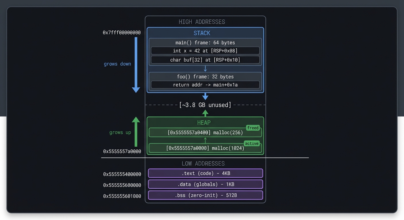
[Press 's' to step, 'c' to continue, 'q' to quit]
The core question you’re answering: How does a running program’s virtual memory map to concrete regions like stack, heap, and code?
Concepts you must understand first:
- Virtual memory maps and segment permissions
- Stack frames and calling conventions
- Heap allocation and fragmentation
- Debugger attach semantics (ptrace or mach)
Questions to guide your design:
- How will you safely attach and read another process’s memory?
- How will you map addresses to regions and names?
- How will you show stack frames and symbols clearly?
Thinking exercise: Take a simple C program and sketch its memory layout while it runs. Where do globals, stack locals, and heap allocations live?
The interview questions they’ll ask:
- What is ASLR and how does it affect memory addresses?
- Why does the stack grow downward on most architectures?
- What permissions are required for ptrace?
- How would you differentiate between heap and mmap allocations?
Hints in layers:
- Hint 1: Start by parsing
/proc/<pid>/mapsand printing regions. - Hint 2: Read
/proc/<pid>/memat a known address to verify access. - Hint 3: Add symbolization with
dladdroraddr2linefor code regions.
Books that will help:
| Topic | Book & Chapter |
|---|---|
| Virtual memory | Computer Systems: A Programmer’s Perspective - Ch. 9 |
| Process memory layout | Computer Systems: A Programmer’s Perspective - Ch. 7 |
| ptrace and debugging | The Linux Programming Interface - Ch. 26 |
Common pitfalls & debugging:
- Problem: Permission denied when attaching.
Why: OS security settings restrict ptrace.
Fix: Adjustptrace_scope(Linux) or run as root.
Quick test: Attach to a process you own. - Problem: Stack frames are wrong or missing.
Why: Optimizations omit frame pointers.
Fix: Compile target with-fno-omit-frame-pointer.
Learning milestones:
- Can read another process’s memory → You understand process isolation and debugging
- Stack visualization shows call frames → You see how functions work at the memory level
- Heap tracking works → You understand dynamic memory allocation
Project 8: x86-64 Disassembler
- File: CPU_ISA_ARCHITECTURE_PROJECTS.md
- Main Programming Language: C
- Alternative Programming Languages: Rust, C++
- Coolness Level: Level 4: Hardcore Tech Flex
- Business Potential: 1. The “Resume Gold” (Educational/Personal Brand)
- Difficulty: Level 4: Expert (The Systems Architect)
- Knowledge Area: ISA Encoding / Reverse Engineering
- Software or Tool: Disassembler
- Main Book: “Computer Systems: A Programmer’s Perspective” by Bryant & O’Hallaron
What you’ll build: A disassembler that reads x86-64 machine code bytes and produces human-readable assembly. Handle common instructions (MOV, ADD, SUB, CMP, JMP, CALL, RET, PUSH, POP).
Why it teaches CPU fundamentals: x86-64 is a CISC architecture with variable-length instructions (1-15 bytes!). Building a disassembler forces you to understand instruction encoding at the deepest level: prefixes, opcodes, ModR/M bytes, SIB bytes, and displacement/immediate fields.
Core challenges you’ll face:
- Decoding variable-length instructions → maps to CISC instruction encoding
- Parsing ModR/M and SIB bytes → maps to addressing mode encoding
- Handling prefixes (REX, operand-size, etc.) → maps to instruction modifiers
- Resolving relative addresses for jumps → maps to PC-relative addressing
Key Concepts:
- x86-64 Instruction Format: “Intel 64 and IA-32 Architectures Software Developer’s Manual” Volume 2 - Intel
- CISC vs RISC: “Computer Organization and Design” Chapter 2.18 - Patterson & Hennessy
- ModR/M Encoding: “Computer Systems: A Programmer’s Perspective” Web Aside ASM:IA32 - Bryant & O’Hallaron
- Disassembly Techniques: “Practical Binary Analysis” Chapter 6 - Dennis Andriesse
Difficulty: Expert Time estimate: 3-4 weeks Prerequisites: 6502 emulator experience, familiarity with x86-64 assembly
Real world outcome:
$ echo -e '\x55\x48\x89\xe5\x48\x83\xec\x10\xc7\x45\xfc\x00\x00\x00\x00\x5d\xc3' | ./disasm
0x0000: 55                 push   rbp
0x0001: 48 89 e5           mov    rbp, rsp
0x0004: 48 83 ec 10        sub    rsp, 0x10
0x0008: c7 45 fc 00 00 00  mov    DWORD PTR [rbp-0x4], 0x0
0x000f: 5d                 pop    rbp
0x0010: c3                 ret

$ ./disasm /bin/ls | head -20
[Disassembly of /bin/ls entry point]
0x4010: 31 ed              xor    ebp, ebp
0x4012: 49 89 d1           mov    r9, rdx
0x4015: 5e                 pop    rsi
0x4016: 48 89 e2           mov    rdx, rsp
...
The core question you’re answering: How do raw bytes become a correct instruction stream in a variable-length ISA?
Concepts you must understand first:
- Instruction prefixes and opcode maps
- ModR/M and SIB addressing encoding
- Immediate and displacement sizes
- PC-relative addressing
Questions to guide your design:
- How will you keep state as you parse variable-length instructions?
- How will you handle ambiguous byte streams and invalid encodings?
- How will you format output consistently?
Thinking exercise: Manually decode a short byte sequence into opcode + operands and verify with an existing disassembler.
The interview questions they’ll ask:
- Why is x86-64 decoding harder than RISC decoding?
- What is the ModR/M byte and what does it encode?
- How do prefixes affect operand size and registers?
- How do you find instruction boundaries in raw bytes?
Hints in layers:
- Hint 1: Build a small opcode table for a subset (MOV/ADD/SUB).
- Hint 2: Parse prefixes first, then opcode, then ModR/M, then SIB/disp/imm.
- Hint 3: Validate length and return an error if bytes run out.
Books that will help:
| Topic | Book & Chapter |
|---|---|
| x86-64 encoding | Intel 64 and IA-32 Manual - Vol. 2 |
| Disassembly basics | Practical Binary Analysis - Ch. 6 |
| ISA overview | Computer Organization and Design - Ch. 2 |
Common pitfalls & debugging:
- Problem: Instructions decode to wrong operands.
Why: ModR/M and SIB fields are misinterpreted.
Fix: Validate each bit field with known examples.
Quick test: Compare output withobjdump -d. - Problem: Decoder desyncs mid-stream.
Why: Instruction length is miscomputed.
Fix: Track bytes consumed per field and assert total length.
Learning milestones:
- Simple instructions (push, pop, ret) decode → You understand basic opcode format
- ModR/M byte parsing works → You understand complex instruction encoding
- Can disassemble real binaries (/bin/ls) → Your disassembler is production-quality
Project 9: Write Programs in Assembly (x86-64 or ARM)
- File: CPU_ISA_ARCHITECTURE_PROJECTS.md
- Main Programming Language: Assembly (x86-64 or ARM64)
- Alternative Programming Languages: x86-64, ARM64, RISC-V
- Coolness Level: Level 4: Hardcore Tech Flex
- Business Potential: 1. The “Resume Gold” (Educational/Personal Brand)
- Difficulty: Level 3: Advanced (The Engineer)
- Knowledge Area: Assembly Programming / Low-level Coding
- Software or Tool: Assembler (nasm, gas)
- Main Book: “Computer Systems: A Programmer’s Perspective” by Bryant & O’Hallaron
What you’ll build: Write real assembly programs: a number printer, string reversal, bubble sort, and finally a simple shell or text editor. No C, no libraries—just raw syscalls.
Why it teaches CPU fundamentals: There’s no substitute for writing assembly. You’ll use registers directly, manage the stack manually, and see exactly what the CPU does. After this, you’ll read compiler output fluently and understand exactly what your C code becomes.
Core challenges you’ll face:
- Making system calls directly (no libc) → maps to user/kernel interface
- Managing registers (caller-saved vs callee-saved) → maps to calling conventions
- Implementing loops and conditionals → maps to branch instructions
- Stack-based local variables → maps to activation records
- String manipulation byte-by-byte → maps to memory access patterns
Key Concepts:
- x86-64 Assembly: “Computer Systems: A Programmer’s Perspective” Chapter 3 - Bryant & O’Hallaron
- System Calls: “The Linux Programming Interface” Chapter 3 - Michael Kerrisk
- Calling Conventions: “Computer Systems: A Programmer’s Perspective” Chapter 3.7 - Bryant & O’Hallaron
- Practical Assembly: “The Art of 64-Bit Assembly, Volume 1” - Randall Hyde
Difficulty: Advanced Time estimate: 2-4 weeks (for multiple programs) Prerequisites: Understanding of registers, stack, basic x86-64 or ARM knowledge
Real world outcome:
; hello.asm - x86-64 Linux
section .data
    msg: db "Hello from raw assembly!", 10
    len: equ $ - msg

section .text
    global _start

_start:
    mov rax, 1          ; sys_write
    mov rdi, 1          ; stdout
    mov rsi, msg        ; buffer
    mov rdx, len        ; length
    syscall

    mov rax, 60         ; sys_exit
    xor rdi, rdi        ; status = 0
    syscall
$ nasm -f elf64 hello.asm && ld hello.o -o hello && ./hello
Hello from raw assembly!

$ wc -c hello
352 hello   # Only 352 bytes! No libc, no bloat.
The core question you’re answering: What does a program look like when you control registers, stack, and syscalls directly?
Concepts you must understand first:
- Calling conventions and ABI rules
- Syscall interfaces and register usage
- Stack alignment and frame setup
- Memory addressing modes in assembly
Questions to guide your design:
- How will you pass arguments to syscalls correctly?
- How will you manage the stack for local data?
- How will you structure control flow without high-level constructs?
Thinking exercise: Write a loop in assembly that sums an array of 10 integers and returns the result in a register.
The interview questions they’ll ask:
- What is the difference between a syscall and a function call?
- Why does the ABI require stack alignment?
- Which registers are caller-saved vs callee-saved?
- How do you implement a switch statement in assembly?
Hints in layers:
- Hint 1: Start with syscalls only (
write,exit) to avoid libc. - Hint 2: Build small macros for common patterns (prologue/epilogue).
- Hint 3: Use a debugger to single-step and inspect registers.
Books that will help:
| Topic | Book & Chapter |
|---|---|
| x86-64 assembly | Computer Systems: A Programmer’s Perspective - Ch. 3 |
| Syscalls and ABI | The Linux Programming Interface - Ch. 3 |
| Practical assembly | The Art of 64-Bit Assembly, Volume 1 |
Common pitfalls & debugging:
- Problem: Program crashes on return.
Why: Stack alignment or return address is corrupted.
Fix: Ensure proper prologue/epilogue and 16-byte alignment.
Quick test: Step intoretand verifyrsp. - Problem: Syscall returns
-EINVAL.
Why: Arguments are in the wrong registers.
Fix: Verify the syscall ABI for your platform.
Learning milestones:
- Hello World works with raw syscalls → You understand the syscall interface
- Bubble sort with loops and array access works → You can write real algorithms
- A simple shell (read command, fork, exec) → You’ve built something useful in pure assembly
Project 10: Game Boy Emulator (Z80-like CPU)
- File: CPU_ISA_ARCHITECTURE_PROJECTS.md
- Main Programming Language: C
- Alternative Programming Languages: Rust, C++
- Coolness Level: Level 5: Pure Magic (Super Cool)
- Business Potential: 1. The “Resume Gold” (Educational/Personal Brand)
- Difficulty: Level 4: Expert (The Systems Architect)
- Knowledge Area: CPU Emulation / Complete System
- Software or Tool: Game Boy Emulator
- Main Book: “Game Boy Coding Adventure” by Maximilien Dagois
What you’ll build: A complete Game Boy emulator: CPU (modified Z80), memory banking, PPU (graphics), timers, and input. Run actual commercial games like Tetris, Pokemon, and Zelda.
Why it teaches CPU fundamentals: The Game Boy is a complete system. The CPU doesn’t exist in isolation—it coordinates with the PPU through memory-mapped registers, handles interrupts, and must run at precise timing. This project shows how all the pieces fit together.
Core challenges you’ll face:
- Implementing the modified Z80 instruction set → maps to full ISA implementation
- Memory banking (switching ROM/RAM banks) → maps to memory management
- Cycle-accurate PPU synchronization → maps to timing and synchronization
- Handling interrupts (VBlank, timer, etc.) → maps to interrupt handling
- Implementing LCD drawing (scanlines, sprites, background) → maps to hardware rendering
Key Concepts:
- Complete CPU Implementation: “Game Boy Coding Adventure” Chapters 3-5 - Maximilien Dagois
- Memory Mapping: “Computer Organization and Design” Chapter 5.2 - Patterson & Hennessy
- Interrupts: “Computer Organization and Design” Chapter 4.9 - Patterson & Hennessy
- Game Boy Specifics: “Pan Docs” (gbdev.io) - The definitive Game Boy technical reference
Difficulty: Expert Time estimate: 1-2 months Prerequisites: 6502 emulator experience, graphics programming basics
Real world outcome:
$ ./gameboy roms/tetris.gb

┌────────────────────────────────────────┐
│          ████████████████              │
│          █  TETRIS     █              │
│          ████████████████              │
│                                        │
│     ██                                 │
│     ██                                 │
│   ████                                 │
│                                        │
│          ████                          │
│          ██                            │
│          ██                            │
│ ────────────────────                  │
│    Score: 1,234                        │
└────────────────────────────────────────┘

Controls: Arrow keys to move, Z to rotate, X to drop
You’re playing the actual Tetris ROM from 1989 on an emulator you built!
The core question you’re answering: How do CPU, graphics, timers, and input coordinate in a real, timing-sensitive system?
Concepts you must understand first:
- Full ISA implementation and instruction timing
- Memory-mapped I/O and register side effects
- Interrupt handling and priority
- Hardware synchronization between CPU and PPU
Questions to guide your design:
- How will you keep CPU cycles and PPU cycles in sync?
- How will you model memory banking and address ranges?
- Which interrupts must be serviced at precise times?
Thinking exercise: Trace a single frame update: CPU executes instructions, triggers VBlank, and PPU renders scanlines.
The interview questions they’ll ask:
- Why are emulators often timing-sensitive rather than just functional?
- What is memory banking and why did the Game Boy need it?
- How do you validate emulation accuracy beyond just “it runs”?
- What is the role of VBlank interrupts?
Hints in layers:
- Hint 1: Implement the CPU core first and pass test ROMs.
- Hint 2: Add memory mapping and timers before full PPU rendering.
- Hint 3: Use logging of cycles per frame to stabilize timing.
Books that will help:
| Topic | Book & Chapter |
|---|---|
| CPU and memory mapping | Computer Organization and Design - Ch. 5 |
| Hardware interrupts | Computer Organization and Design - Ch. 4 |
| Game Boy specifics | Game Boy Coding Adventure - Ch. 3-5 |
Common pitfalls & debugging:
- Problem: Games boot but crash after a few seconds.
Why: Timer or interrupt timing is incorrect.
Fix: Tie interrupts to cycle counts and verify against test ROMs.
Quick test: Use Blargg’s timing tests. - Problem: Graphics flicker or distort.
Why: PPU scanline timing is off.
Fix: Advance PPU state based on CPU cycles.
Learning milestones:
- CPU passes Blargg’s test ROMs → Your CPU is accurate
- Simple games boot and are playable → CPU + PPU + input work together
- Pokemon runs → You’ve handled edge cases and complex memory banking
Project 11: Bare-Metal Programming (Raspberry Pi or Arduino)
- File: CPU_ISA_ARCHITECTURE_PROJECTS.md
- Main Programming Language: C with inline Assembly
- Alternative Programming Languages: Rust, Assembly-only
- Coolness Level: Level 5: Pure Magic (Super Cool)
- Business Potential: 1. The “Resume Gold” (Educational/Personal Brand)
- Difficulty: Level 4: Expert (The Systems Architect)
- Knowledge Area: Bare-Metal / Operating Systems
- Software or Tool: Bare-metal Raspberry Pi / Arduino
- Main Book: “Computer Systems: A Programmer’s Perspective” by Bryant & O’Hallaron
What you’ll build: A program that runs on a Raspberry Pi with NO operating system. You’ll boot directly into your code, blink an LED, read a button, and output text over UART—all by directly accessing hardware registers.
Why it teaches CPU fundamentals: With no OS, there’s nothing between you and the CPU. You’ll configure the hardware by writing to memory-mapped registers, handle interrupts yourself, and see exactly how the CPU boots. This is the ultimate understanding of how computers really work.
Core challenges you’ll face:
- Writing a bootloader/linker script → maps to how programs are loaded into memory
- Configuring GPIO by writing to registers → maps to memory-mapped I/O
- Implementing busy-wait and timer-based delays → maps to hardware timers
- Setting up UART for serial output → maps to peripheral communication
- Handling interrupts without an OS → maps to interrupt vectors and handlers
Key Concepts:
- Bootloaders and Linker Scripts: “Making Embedded Systems” Chapter 3 - Elecia White
- Memory-Mapped I/O: “Computer Organization and Design” Chapter 5.2 - Patterson & Hennessy
- Bare-Metal Setup: “Bare Metal C” Chapters 1-5 - Steve Oualline
- ARM Specifics: “The Art of ARM Assembly, Volume 1” - Randall Hyde
Difficulty: Expert Time estimate: 2-4 weeks Prerequisites: C programming, basic electronics, previous emulator experience
Real world outcome:
// main.c - No OS, no libraries, just you and the hardware
#include "gpio.h"
#include "uart.h"

void kernel_main() {
    uart_init();
    uart_puts("Hello from bare metal!\r\n");

    gpio_set_function(47, GPIO_FUNC_OUTPUT);  // LED pin

    while (1) {
        gpio_set(47);            // LED on
        delay_ms(500);
        gpio_clear(47);          // LED off
        delay_ms(500);
        uart_puts("Blink!\r\n");
    }
}
$ arm-none-eabi-gcc -nostdlib -ffreestanding kernel.c -o kernel.elf
$ arm-none-eabi-objcopy kernel.elf -O binary kernel8.img
$ # Copy to SD card, insert in Raspberry Pi, power on

[UART output via serial cable]:
Hello from bare metal!
Blink!
Blink!
Blink!
The LED blinks. No Linux. No OS. Just your code running directly on the CPU.
The core question you’re answering: What must a CPU do to boot and interact with hardware when there is no operating system?
Concepts you must understand first:
- Reset vectors and boot sequences
- Memory-mapped I/O registers
- Linker scripts and memory layout
- Interrupt vectors and handlers
Questions to guide your design:
- Where will your code live in memory after reset?
- How will you initialize the stack and
.bss? - Which peripherals require clock or pin configuration?
Thinking exercise: Map out the first 10 instructions that run after reset and explain how the stack becomes valid.
The interview questions they’ll ask:
- Why must MMIO registers be declared
volatile? - What is the difference between a boot ROM and a bootloader?
- How do interrupts work without an OS?
- What can go wrong if caches are enabled too early?
Hints in layers:
- Hint 1: Start with a minimal linker script and a
_startentry. - Hint 2: Implement UART output first for debug visibility.
- Hint 3: Add GPIO toggling once you can print and delay reliably.
Books that will help:
| Topic | Book & Chapter |
|---|---|
| Bare-metal workflow | Bare Metal C - Ch. 1-5 |
| Embedded boot flow | Making Embedded Systems - Ch. 3 |
| MMIO and peripherals | Computer Organization and Design - Ch. 5 |
Common pitfalls & debugging:
- Problem: Nothing prints over UART.
Why: UART clock/pin configuration is missing.
Fix: Enable peripheral clocks and set pin function.
Quick test: Read back UART status registers. - Problem: Program crashes after enabling interrupts.
Why: Vector table or stack is not initialized.
Fix: Set vector base and initialize stack beforecpsie i.
Learning milestones:
- LED blinks → You can control hardware directly
- UART output works → You’ve configured a peripheral from scratch
- Button input with interrupts → You understand interrupt handling without an OS
Project 12: RISC-V CPU on FPGA
- File: CPU_ISA_ARCHITECTURE_PROJECTS.md
- Main Programming Language: Verilog or VHDL
- Alternative Programming Languages: Verilog, VHDL, Chisel
- Coolness Level: Level 5: Pure Magic (Super Cool)
- Business Potential: 1. The “Resume Gold” (Educational/Personal Brand)
- Difficulty: Level 5: Master (The First-Principles Wizard)
- Knowledge Area: CPU Design / Digital Logic
- Software or Tool: FPGA (Lattice iCE40, Xilinx Artix)
- Main Book: “Digital Design and Computer Architecture” by Harris & Harris
What you’ll build: A real CPU implemented in hardware (Verilog/VHDL) running on an FPGA. Implement the RISC-V RV32I instruction set, write programs in RISC-V assembly, and watch them execute on your CPU.
Why it teaches CPU fundamentals: This is the ultimate project. You’re not emulating a CPU in software—you’re building one in actual hardware. You’ll implement registers as flip-flops, the ALU as combinational logic, and the control unit as a state machine. After this, you truly understand CPUs at the transistor level.
Core challenges you’ll face:
- Implementing a register file in Verilog → maps to storage elements
- Building an ALU with carry chains → maps to arithmetic circuits
- Designing the control unit (FSM or hardwired) → maps to control signals
- Memory interface (BRAM, load/store) → maps to memory hierarchy
- Pipelining (optional, advanced) → maps to CPU performance optimization
Key Concepts:
- Digital Logic in Verilog: “Digital Design and Computer Architecture” Chapters 1-4 - Harris & Harris
- CPU Datapath: “Computer Organization and Design RISC-V Edition” Chapter 4.3 - Patterson & Hennessy
- Control Unit Design: “Computer Organization and Design RISC-V Edition” Chapter 4.4 - Patterson & Hennessy
- FPGA Workflow: “Getting Started with FPGAs” - Russell Merrick
Difficulty: Master Time estimate: 2-3 months Prerequisites: Digital logic, previous emulator experience, basic Verilog/VHDL
Real world outcome:
// A snippet of your CPU in Verilog
module cpu (
    input wire clk,
    input wire reset,
    output wire [31:0] pc_out,
    output wire [31:0] instr_out
);
    reg [31:0] pc;
    reg [31:0] regs [0:31];
    wire [31:0] instruction;

    // Fetch
    assign instruction = imem[pc[9:2]];

    // Decode
    wire [6:0] opcode = instruction[6:0];
    wire [4:0] rd = instruction[11:7];
    wire [4:0] rs1 = instruction[19:15];

    // Execute (ALU)
    // ... your implementation here
endmodule
$ yosys -p "synth_ice40" cpu.v        # Synthesize
$ nextpnr-ice40 --hx8k cpu.json       # Place & Route
$ icepack cpu.asc cpu.bin             # Generate bitstream
$ iceprog cpu.bin                     # Program FPGA

[LEDs on FPGA board show program counter advancing]
[UART output]: Running Fibonacci on YOUR CPU!
F(10) = 55
You’ve built a real CPU. In hardware. That runs programs.
The core question you’re answering: How do abstract ISA rules become real flip-flops, wires, and clocked logic?
Concepts you must understand first:
- Combinational vs sequential logic
- Register files and writeback timing
- ALU control signals and muxing
- FSM-based control vs hardwired control
Questions to guide your design:
- Will you build a single-cycle or multi-cycle CPU first?
- How will you separate datapath and control?
- How will you test correctness before hardware deployment?
Thinking exercise: Draw the datapath for ADD x3, x1, x2 and label every mux and control signal involved.
The interview questions they’ll ask:
- Why do multi-cycle designs reduce hardware complexity?
- What is the critical path in a single-cycle CPU?
- How do you implement a register file in Verilog?
- What changes when you add pipelining?
Hints in layers:
- Hint 1: Start with RV32I subset:
ADD,SUB,LW,SW,BEQ,JAL. - Hint 2: Write a simple testbench that runs a small program.
- Hint 3: Use waveform tools to verify control signals per instruction.
Books that will help:
| Topic | Book & Chapter |
|---|---|
| Datapath and control | Computer Organization and Design (RISC-V Edition) - Ch. 4 |
| Verilog logic design | Digital Design and Computer Architecture - Ch. 1-5 |
| FPGA workflow | Getting Started with FPGAs - Russell Merrick |
Common pitfalls & debugging:
- Problem: CPU works in simulation but fails on FPGA.
Why: Clock/reset or timing constraints are wrong.
Fix: Add proper reset synchronization and constraints.
Quick test: Blink an LED driven by the clock divider. - Problem: Incorrect register values after ALU ops.
Why: Writeback timing or mux select is wrong.
Fix: Trace writeback signals and verify per instruction.
Learning milestones:
- Basic instructions execute in simulation → Your Verilog describes a working CPU
- Runs on actual FPGA hardware → Your design maps to real logic gates
- Runs programs you wrote in RISC-V assembly → You have a complete, working CPU you designed
Project 13: CPU Pipeline Simulator
- File: CPU_ISA_ARCHITECTURE_PROJECTS.md
- Main Programming Language: C
- Alternative Programming Languages: Rust, Python, C++
- Coolness Level: Level 3: Genuinely Clever
- Business Potential: 1. The “Resume Gold” (Educational/Personal Brand)
- Difficulty: Level 3: Advanced (The Engineer)
- Knowledge Area: CPU Performance / Pipelining
- Software or Tool: Pipeline Visualizer
- Main Book: “Computer Organization and Design” by Patterson & Hennessy
What you’ll build: A simulator that shows how a pipelined CPU executes instructions. Visualize the 5-stage pipeline (IF, ID, EX, MEM, WB), show hazards, forwarding, stalls, and branch prediction.
Why it teaches CPU fundamentals: Modern CPUs don’t execute one instruction at a time—they overlap many instructions in a pipeline. Understanding hazards (data, control, structural) and how CPUs solve them (forwarding, stalling, speculation) is essential for writing fast code.
Core challenges you’ll face:
- Implementing 5 pipeline stages → maps to pipelining basics
- Detecting data hazards (RAW, WAR, WAW) → maps to dependency analysis
- Implementing forwarding/bypassing → maps to hazard mitigation
- Branch prediction (static, dynamic) → maps to control hazards
- Calculating CPI (Cycles Per Instruction) → maps to performance metrics
Key Concepts:
- Pipelining: “Computer Organization and Design” Chapter 4.5-4.8 - Patterson & Hennessy
- Hazards: “Computer Organization and Design” Chapter 4.7 - Patterson & Hennessy
- Branch Prediction: “Computer Architecture” Chapter 3.3 - Hennessy & Patterson
- Performance: “Computer Organization and Design” Chapter 1.6 - Patterson & Hennessy
Difficulty: Advanced Time estimate: 2-3 weeks Prerequisites: Understanding of basic CPU operation, emulator experience
Real world outcome:
$ ./pipelinesim program.asm

Clock Cycle: 10
┌───────┬───────┬───────┬───────┬───────┐
│  IF   │  ID   │  EX   │  MEM  │  WB   │
├───────┼───────┼───────┼───────┼───────┤
│ ADD   │ LW    │ SUB   │ MUL   │ ADD   │
│ R5,R6 │ R3,0( │ R4,R1 │ R2,R1 │ R1,R2 │
│ ,R7   │ R2)   │ ,R3   │ ,R3   │ ,R3   │
└───────┴───────┴───────┴───────┴───────┘

Hazard Detected: RAW on R3 between LW and SUB
Action: Forwarding from MEM/WB to EX stage

Stats:
- Instructions: 100
- Cycles: 134
- CPI: 1.34
- Stalls due to load-use: 12
- Branch mispredictions: 5
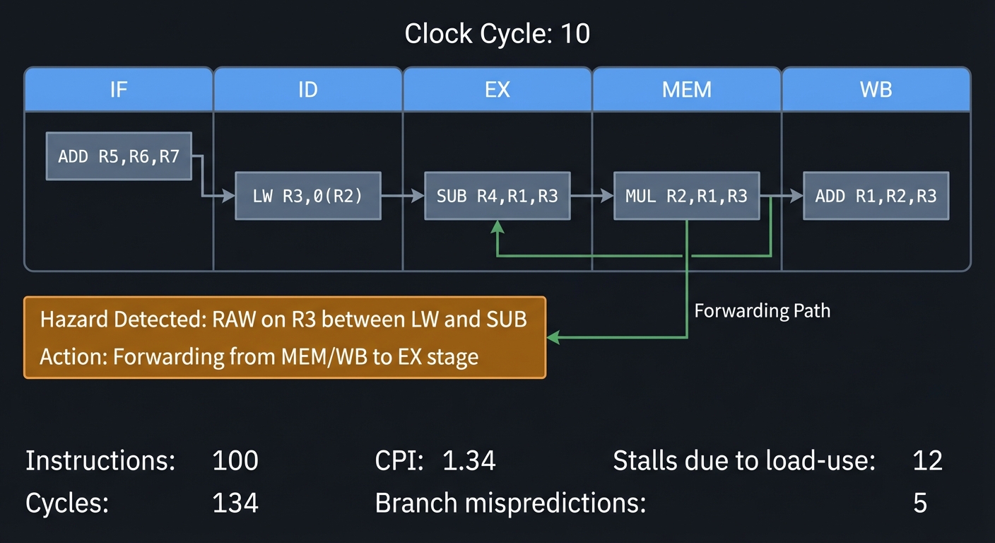
The core question you’re answering: How does overlapping instruction execution change correctness and performance?
Concepts you must understand first:
- Pipeline stages and register boundaries
- Data and control hazards
- Forwarding and stalling logic
- Branch prediction basics
Questions to guide your design:
- How will you represent the pipeline state per stage?
- When does an instruction need to stall or be flushed?
- How will you compute CPI and cycle counts?
Thinking exercise: Take a 5-instruction sequence with a load-use hazard and draw the pipeline timeline with stalls.
The interview questions they’ll ask:
- What is the difference between throughput and latency in a pipeline?
- How does forwarding resolve RAW hazards?
- Why do branches cause bubbles?
- What is the ideal CPI and why is it rarely achieved?
Hints in layers:
- Hint 1: Simulate stage registers explicitly (IF/ID, ID/EX, EX/MEM, MEM/WB).
- Hint 2: Start with no hazards, then add hazard detection rules.
- Hint 3: Add a trace mode that prints the pipeline each cycle.
Books that will help:
| Topic | Book & Chapter |
|---|---|
| Pipelining fundamentals | Computer Organization and Design - Ch. 4 |
| Hazards and forwarding | Computer Organization and Design - Ch. 4.7 |
| Branch prediction | Computer Architecture - Ch. 3 |
Common pitfalls & debugging:
- Problem: Instructions complete out of order incorrectly.
Why: Writeback or forwarding is misapplied.
Fix: Validate dependencies and ensure correct bypassing.
Quick test: Use a small program with known results. - Problem: Branches never resolve correctly.
Why: PC update timing is wrong.
Fix: Define exactly when branch decision is made and flush younger stages.
Learning milestones:
- Instructions flow through 5 stages → You understand basic pipelining
- Hazards are detected and displayed → You understand dependencies
- Performance metrics match expected values → You can analyze CPU efficiency
Project 14: Cache Simulator
- File: CPU_ISA_ARCHITECTURE_PROJECTS.md
- Main Programming Language: C
- Alternative Programming Languages: Rust, C++, Python
- Coolness Level: Level 3: Genuinely Clever
- Business Potential: 1. The “Resume Gold” (Educational/Personal Brand)
- Difficulty: Level 3: Advanced (The Engineer)
- Knowledge Area: Memory Hierarchy / Caching
- Software or Tool: Cache Simulator
- Main Book: “Computer Systems: A Programmer’s Perspective” by Bryant & O’Hallaron
What you’ll build: A cache simulator that models L1, L2, and L3 caches. Feed it memory access traces and see hit rates, eviction patterns, and how different configurations affect performance.
Why it teaches CPU fundamentals: Memory is the bottleneck. CPUs spend more time waiting for memory than computing. Understanding caches—how they work, why they help, and how to write cache-friendly code—is essential for performance.
Core challenges you’ll face:
- Implementing direct-mapped, set-associative, fully-associative caches → maps to cache organization
- Address parsing (tag, index, offset) → maps to how addresses map to cache lines
- Replacement policies (LRU, FIFO, random) → maps to eviction strategies
- Multi-level cache hierarchy → maps to modern memory systems
- Write policies (write-through, write-back) → maps to cache coherence basics
Key Concepts:
- Cache Organization: “Computer Systems: A Programmer’s Perspective” Chapter 6.3-6.4 - Bryant & O’Hallaron
- Locality: “Computer Systems: A Programmer’s Perspective” Chapter 6.2 - Bryant & O’Hallaron
- Multi-level Caches: “Computer Organization and Design” Chapter 5.8 - Patterson & Hennessy
- Cache Performance: “Computer Systems: A Programmer’s Perspective” Chapter 6.6 - Bryant & O’Hallaron
Difficulty: Advanced Time estimate: 2 weeks Prerequisites: Understanding of memory addressing, basic C
Real world outcome:
$ ./cachesim --l1-size=32K --l1-assoc=8 --line=64 trace.txt

Simulating cache access for 1,000,000 memory references...

Cache Configuration:
  L1: 32KB, 8-way set-associative, 64-byte lines
  L2: 256KB, 16-way set-associative, 64-byte lines

Results:
┌─────────┬───────────┬───────────┬───────────┐
│  Cache  │   Hits    │  Misses   │ Hit Rate  │
├─────────┼───────────┼───────────┼───────────┤
│   L1    │  920,145  │   79,855  │   92.0%   │
│   L2    │   71,234  │    8,621  │   89.2%   │
│  Memory │    8,621  │     -     │     -     │
└─────────┴───────────┴───────────┴───────────┘

Average Memory Access Time: 4.3 cycles
(vs. ~100 cycles if no cache!)

Hottest cache lines:
  0x7fff5a00: 15,234 hits (loop counter)
  0x5555b040: 8,456 hits (frequently accessed array)
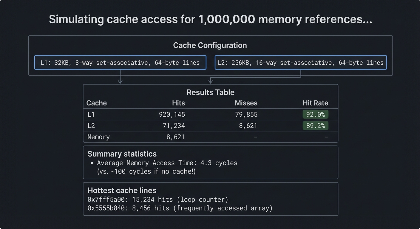
The core question you’re answering: How does data locality translate into real performance improvements?
Concepts you must understand first:
- Cache line, set, and tag structure
- Mapping strategies and associativity
- Replacement and write policies
- Temporal and spatial locality
Questions to guide your design:
- How will you split addresses into tag/index/offset?
- Which replacement policy will you implement first?
- How will you validate hit/miss behavior?
Thinking exercise: Take a small loop over an array and predict the hit rate for a 64-byte cache line.
The interview questions they’ll ask:
- Why does increasing associativity reduce conflict misses?
- What is the difference between write-through and write-back?
- How do caches exploit spatial locality?
- Why can a small cache beat a large one for some workloads?
Hints in layers:
- Hint 1: Implement direct-mapped cache first.
- Hint 2: Add LRU with a small counter per set.
- Hint 3: Feed in a trace from a simple program and compare results with expectations.
Books that will help:
| Topic | Book & Chapter |
|---|---|
| Cache organization | Computer Systems: A Programmer’s Perspective - Ch. 6 |
| Memory hierarchy | Computer Organization and Design - Ch. 5 |
| Performance metrics | Computer Architecture - Ch. 3 |
Common pitfalls & debugging:
- Problem: Hit rates are too high or too low.
Why: Address decomposition is incorrect.
Fix: Verify tag/index/offset bit widths.
Quick test: Use a trace with a known pattern (sequential). - Problem: LRU behaves randomly.
Why: You are not updating access order consistently.
Fix: Update LRU on every hit and miss.
Learning milestones:
- Direct-mapped cache works → You understand basic cache mechanics
- Set-associative with LRU works → You understand realistic cache design
- Multi-level hierarchy shows realistic behavior → You understand modern memory systems
Project 15: Branch Predictor Simulator
- File: CPU_ISA_ARCHITECTURE_PROJECTS.md
- Main Programming Language: C
- Alternative Programming Languages: Rust, C++, Python
- Coolness Level: Level 3: Genuinely Clever
- Business Potential: 1. The “Resume Gold” (Educational/Personal Brand)
- Difficulty: Level 3: Advanced (The Engineer)
- Knowledge Area: CPU Performance / Branch Prediction
- Software or Tool: Branch Predictor Simulator
- Main Book: “Computer Architecture” by Hennessy & Patterson
What you’ll build: A simulator that implements various branch prediction algorithms: static (always taken/not-taken), 1-bit, 2-bit saturating counters, and more advanced schemes like gshare and tournament predictors.
Why it teaches CPU fundamentals: Branch mispredictions are expensive—they flush the pipeline and waste cycles. Modern CPUs have sophisticated predictors with 95%+ accuracy. Understanding prediction helps you write code that CPUs can predict well.
Core challenges you’ll face:
- Implementing 2-bit saturating counters → maps to local branch history
- Implementing gshare (global history XOR) → maps to global branch prediction
- Tournament predictor (choosing between predictors) → maps to hybrid schemes
- Analyzing misprediction patterns → maps to understanding CPU performance
Key Concepts:
- Branch Prediction Basics: “Computer Organization and Design” Chapter 4.8 - Patterson & Hennessy
- Dynamic Prediction: “Computer Architecture” Chapter 3.3 - Hennessy & Patterson
- Tournament Predictors: “Computer Architecture” Chapter 3.3 - Hennessy & Patterson
- Real-World Predictors: Academic papers on TAGE, neural branch prediction
Difficulty: Advanced Time estimate: 1-2 weeks Prerequisites: Understanding of pipelining, control hazards
Real world outcome:
$ ./branchsim --predictor=gshare --history=12 trace.txt

Branch Predictor Comparison (1M branches):

┌──────────────────────┬───────────────┬──────────────┐
│      Predictor       │  Accuracy (%) │ Mispredicts  │
├──────────────────────┼───────────────┼──────────────┤
│ Always Taken         │     62.3%     │   377,000    │
│ 1-bit Local          │     85.1%     │   149,000    │
│ 2-bit Saturating     │     91.2%     │    88,000    │
│ Gshare (12-bit)      │     95.4%     │    46,000    │
│ Tournament           │     96.1%     │    39,000    │
└──────────────────────┴───────────────┴──────────────┘

If pipeline is 15 stages deep, misprediction cost = ~15 cycles
Cycles saved by 2-bit vs Always-Taken: 4,335,000 cycles!

Branch patterns detected:
- Loop branches: 98.2% predictable (taken N-1 times, then not taken)
- Data-dependent branches: 73.4% predictable (biased toward taken)
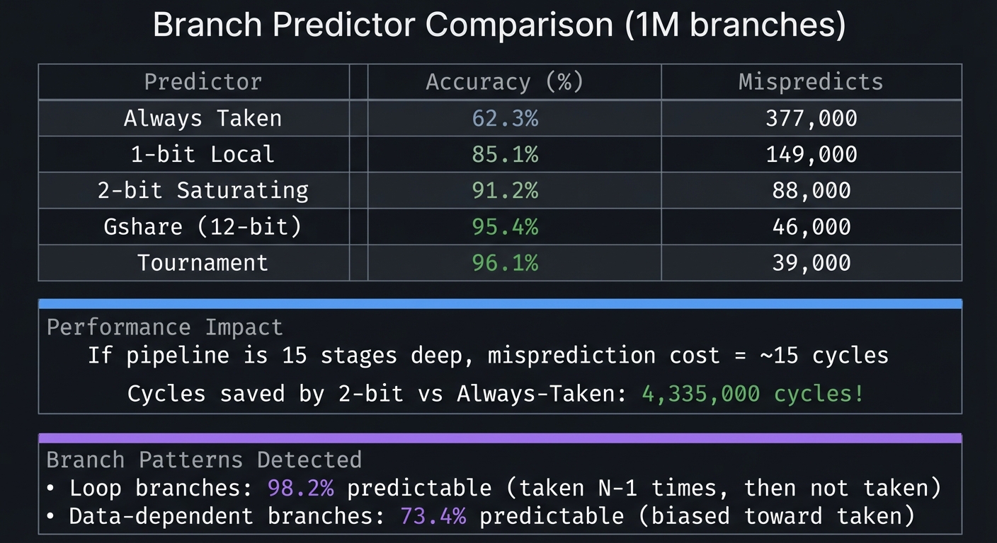
The core question you’re answering: How can a CPU predict the future to keep pipelines full?
Concepts you must understand first:
- Control hazards and pipeline flushing
- Local vs global branch history
- 2-bit saturating counters
- Correlation and predictor selection
Questions to guide your design:
- How will you index prediction tables (PC, history, or both)?
- How will you update predictor state on mispredicts?
- How will you measure accuracy and cost?
Thinking exercise: Take a loop that iterates N times and predict the outcome sequence for 1-bit vs 2-bit predictors.
The interview questions they’ll ask:
- Why are 2-bit predictors more stable than 1-bit?
- What is gshare and why does XOR help?
- What is a tournament predictor?
- How do branch mispredicts affect CPI?
Hints in layers:
- Hint 1: Start with an always-taken baseline for comparison.
- Hint 2: Implement 2-bit counters in a small table indexed by lower PC bits.
- Hint 3: Add global history and gshare once local works.
Books that will help:
| Topic | Book & Chapter |
|---|---|
| Branch prediction | Computer Architecture - Ch. 3 |
| Control hazards | Computer Organization and Design - Ch. 4 |
| Performance analysis | Computer Architecture - Ch. 3 |
Common pitfalls & debugging:
- Problem: Predictor accuracy is unrealistically high.
Why: You are training on the same data you evaluate.
Fix: Separate warmup/training and evaluation phases.
Quick test: Use two different trace files. - Problem: gshare behaves worse than local predictor.
Why: History length is too long or indexing is wrong.
Fix: Try smaller history lengths and verify indexing.
Learning milestones:
- 2-bit predictor beats 1-bit → You understand why state machines help
- Gshare beats local predictors → You understand global correlation
- You can analyze code for predictability → You write CPU-friendly code
Project Comparison Table
| # | Project | Difficulty | Time | Depth of Understanding | Coolness |
|---|---|---|---|---|---|
| 1 | Binary/Hex Visualizer | Beginner | Weekend | ⭐⭐ | ⭐⭐ |
| 2 | Logic Gate Simulator | Beginner | 1 week | ⭐⭐⭐ | ⭐⭐⭐ |
| 3 | Stack Machine VM | Intermediate | 1 week | ⭐⭐⭐ | ⭐⭐⭐ |
| 4 | CHIP-8 Emulator | Intermediate | 1-2 weeks | ⭐⭐⭐⭐ | ⭐⭐⭐⭐ |
| 5 | Custom RISC CPU | Advanced | 2-3 weeks | ⭐⭐⭐⭐⭐ | ⭐⭐⭐⭐ |
| 6 | 6502 Emulator | Advanced | 3-4 weeks | ⭐⭐⭐⭐⭐ | ⭐⭐⭐⭐⭐ |
| 7 | Memory Visualizer | Advanced | 2-3 weeks | ⭐⭐⭐⭐ | ⭐⭐⭐ |
| 8 | x86-64 Disassembler | Expert | 3-4 weeks | ⭐⭐⭐⭐⭐ | ⭐⭐⭐⭐ |
| 9 | Assembly Programming | Advanced | 2-4 weeks | ⭐⭐⭐⭐⭐ | ⭐⭐⭐⭐ |
| 10 | Game Boy Emulator | Expert | 1-2 months | ⭐⭐⭐⭐⭐ | ⭐⭐⭐⭐⭐ |
| 11 | Bare-Metal RPi | Expert | 2-4 weeks | ⭐⭐⭐⭐⭐ | ⭐⭐⭐⭐⭐ |
| 12 | RISC-V on FPGA | Master | 2-3 months | ⭐⭐⭐⭐⭐ | ⭐⭐⭐⭐⭐ |
| 13 | Pipeline Simulator | Advanced | 2-3 weeks | ⭐⭐⭐⭐ | ⭐⭐⭐ |
| 14 | Cache Simulator | Advanced | 2 weeks | ⭐⭐⭐⭐ | ⭐⭐⭐ |
| 15 | Branch Predictor | Advanced | 1-2 weeks | ⭐⭐⭐⭐ | ⭐⭐⭐ |
Final Capstone Project: Full System-on-Chip
After completing the learning path, tackle this ultimate project:
Project: RISC-V System-on-Chip with Peripherals
- File: CPU_ISA_ARCHITECTURE_PROJECTS.md
- Main Programming Language: Verilog + C (for firmware)
- Alternative Programming Languages: VHDL + Rust, Chisel + C
- Coolness Level: Level 5: Pure Magic (Super Cool)
- Business Potential: 1. The “Resume Gold” (Educational/Personal Brand)
- Difficulty: Level 5: Master (The First-Principles Wizard)
- Knowledge Area: CPU Design / System Integration
- Software or Tool: FPGA + Peripherals
- Main Book: “Computer Organization and Design RISC-V Edition” by Patterson & Hennessy
What you’ll build: A complete RISC-V CPU on an FPGA with: UART for serial communication, GPIO for LED/button control, a timer peripheral, interrupt controller, and SRAM interface. Write a bootloader and simple OS kernel that runs on YOUR CPU.
Why this is the capstone: This combines everything: you design the CPU, the memory interface, the peripherals, the interrupt handling, AND the software. When you boot Linux on a CPU you designed, you’ve reached the summit.
Core challenges you’ll face:
- Multi-stage pipeline with forwarding → maps to everything from previous projects
- Memory-mapped peripheral bus (Wishbone or AXI-Lite) → maps to bus protocols
- Interrupt controller (PLIC) → maps to interrupt prioritization
- Writing a bootloader in assembly → maps to system initialization
- Device drivers for your peripherals → maps to hardware/software interface
Key Concepts:
- SoC Design: “Digital Design and Computer Architecture” Chapter 8 - Harris & Harris
- Bus Protocols: “Computer Organization and Design” Chapter 5 - Patterson & Hennessy
- Interrupt Handling: “Computer Organization and Design” Chapter 4.9 - Patterson & Hennessy
- RISC-V Privileged Spec: Official RISC-V Privileged Architecture specification
Difficulty: Master Time estimate: 3-4 months Prerequisites: All previous projects, especially RISC-V on FPGA and bare-metal programming
Real world outcome:
[FPGA UART output]
=====================================
   MY RISC-V SoC v1.0
   CPU: RV32I @ 50MHz
   RAM: 64KB SRAM
   Peripherals: UART, GPIO, Timer
=====================================

Bootloader loaded. Starting kernel...

[MyOS]> gpio led on
LED is now ON

[MyOS]> timer 1000
Setting timer for 1000ms...
[IRQ] Timer interrupt! 1000ms elapsed.

[MyOS]> cat hello.txt
Hello from my CPU!

[MyOS]> run fibonacci
F(20) = 6765 (computed in 234 cycles)
The core question you’re answering: How do you integrate CPU, memory, and peripherals into a coherent, bootable computer system?
Concepts you must understand first:
- Memory maps and bus protocols (AXI-lite/Wishbone)
- Interrupt controllers and prioritization
- Boot ROM, bootloader, and kernel handoff
- Device drivers and MMIO register design
Questions to guide your design:
- What address ranges belong to RAM vs peripherals?
- How will devices raise and clear interrupts?
- What is the minimal firmware to prove the system works?
Thinking exercise: Design a full memory map on paper (ROM, RAM, UART, GPIO, timer) and describe the initialization order.
The interview questions they’ll ask:
- What is the difference between a CPU core and an SoC?
- Why are bus protocols important for integration?
- How do you handle interrupt storms or priority inversion?
- What is the difference between polling and interrupt-driven I/O?
Hints in layers:
- Hint 1: Start with a simple memory map and a UART-only peripheral.
- Hint 2: Add a timer peripheral and a basic interrupt controller.
- Hint 3: Write a tiny monitor shell to verify every peripheral interactively.
Books that will help:
| Topic | Book & Chapter |
|---|---|
| SoC integration | Digital Design and Computer Architecture - Ch. 8 |
| Bus and memory system | Computer Organization and Design - Ch. 5 |
| Embedded firmware | Making Embedded Systems - Ch. 4-6 |
Common pitfalls & debugging:
- Problem: CPU hangs after enabling interrupts.
Why: Interrupt vectors or ACK logic are incorrect.
Fix: Verify vector addresses and acknowledge sequence.
Quick test: Trigger a single timer IRQ and verify handler entry/exit. - Problem: Peripherals respond but data is corrupted.
Why: Bus timing or width mismatches.
Fix: Align data widths and add wait-state logic if needed.
You’ve built a complete computer. From logic gates to running programs. This is what understanding CPUs looks like.
Essential Resources
Primary Books (in order of importance)
- “Code: The Hidden Language” by Charles Petzold - Start here. No prerequisites.
- “Computer Systems: A Programmer’s Perspective” by Bryant & O’Hallaron - The programmer’s view.
- “Computer Organization and Design RISC-V Edition” by Patterson & Hennessy - The hardware view.
- “Digital Design and Computer Architecture” by Harris & Harris - For FPGA work.
Online References
- Nand2Tetris (nand2tetris.org) - Build a computer from logic gates to Tetris
- Ben Eater’s YouTube - 8-bit breadboard computer, visual explanations
- RISC-V Specifications (riscv.org) - Official ISA documentation
- Pan Docs (gbdev.io) - Game Boy technical reference
Tools You’ll Need
- C Compiler: GCC or Clang
- Assembler: NASM (x86-64), GNU as, or RISC-V toolchain
- Emulator Testing: Existing emulators to compare against
- FPGA: iCE40 boards (~$50) for hardware projects
- Raspberry Pi: For bare-metal projects
Start with Project 1. The journey of understanding CPUs begins with understanding that everything is just bits.