ARM Assembly Mastery - Real World Projects
Goal: Build a first-principles understanding of ARM assembly across microcontrollers and application-class systems, with enough depth to reason about performance, correctness, and hardware behavior. You will internalize how ARM profiles, execution states, registers, and memory maps shape the machine-level reality beneath high-level code, and how toolchains turn assembly into runnable binaries. You will be able to analyze and explain boot flows, interrupts, calling conventions, and memory ordering, and you will build real, observable projects that validate each concept. By the end, you can navigate both Cortex-M (Thumb) and AArch64 worlds with confidence and produce artifacts that prove you understand how ARM systems actually work.
Introduction
- What is ARM assembly? It is the human-readable form of the instructions that ARM CPUs execute. ARM is a family of architectures with multiple profiles (A, M, R), each optimized for different constraints and use cases. citeturn0search0turn0search1turn0search2
- What problem does it solve today? It gives you control and insight over performance, timing, and hardware interaction in environments where abstractions leak: microcontrollers, real-time systems, firmware, OS kernels, and low-level tooling.
- What will you build? A toolchain explorer, instruction encoder/decoder, register and stack visualizer, vector table builder, interrupt-driven I/O demos, ABI audits, memory-ordering litmus tests, and a capstone bare-metal monitor.
- In scope vs out of scope: In scope are ARMv6-M/ARMv7-M (Thumb) and ARMv8-A (AArch64) concepts, toolchains, and bare-metal workflows. Out of scope are high-level OS driver frameworks, full Linux kernel bring-up, and vendor-specific BSPs (you will reference them, but not depend on them).
Big Picture: Why ARM Assembly Matters
─────────────────────────────────────────────────────────────────────────
Apps/OS code ─▶ Compiler ─▶ ARM ISA ─▶ Registers/Memory ─▶ Peripherals
     ^                  ^         ^            ^               ^
     |                  |         |            |               |
Readability         Toolchain  Instruction  Boot/Interrupts  MMIO
                   choices     encoding      & exceptions     timing
How to Use This Guide
- Read the Theory Primer first; it is the mental model that makes the projects meaningful.
- Pick a learning path that fits your target: Cortex-M (embedded) or AArch64 (systems).
- Treat each project as an experiment: define the expected outcome, build it, then verify.
Prerequisites & Background Knowledge
Essential Prerequisites (Must Have)
- Comfortable with C or Rust at the level of pointers, structs, and function calls.
- Binary/hex conversions and bitwise operations.
- Basic CPU concepts: registers, memory, stack, and instruction execution.
- Recommended Reading: “Computer Organization and Design: ARM Edition” by Patterson & Hennessy - Ch. 1-3.
Helpful But Not Required
- Familiarity with Linux command-line tooling (objdump, readelf, gdb).
- Prior microcontroller exposure (GPIO, UART) or Raspberry Pi bring-up.
Self-Assessment Questions
- Can you explain the difference between a register and a memory address?
- Can you convert 0b10110100 to hex without a calculator?
- Can you describe what happens when a function call returns?
Development Environment Setup Required Tools:
- GNU binutils (as, ld, objdump, readelf) - recent version. citeturn1search1
- AArch64 toolchain (cross-compiler or assembler) - recent version.
Recommended Tools:
- QEMU for ARM emulation.
- OpenOCD + GDB for hardware debugging.
Testing Your Setup: $ aarch64-none-elf-as –version GNU assembler (aarch64-unknown-elf) version X.Y
Time Investment
- Simple projects: 4-8 hours each
- Moderate projects: 10-20 hours each
- Complex projects: 20-40 hours each
- Total sprint: 2-4 months
Important Reality Check ARM assembly exposes details that most developers never see. Expect to be slow at first; speed and intuition only come after repeated, observable experiments.
Big Picture / Mental Model
ARM assembly is not a single language. It is a family of instruction sets and conventions that map to the same architectural lineage but diverge by profile and execution state. A mental model that connects architecture → registers → memory map → toolchain is what makes the projects coherent.
Mental Model: From Architecture to Observable Behavior
─────────────────────────────────────────────────────────────────────────
Architecture Profile (A/M/R)
         │
         ├── Execution State (AArch64 / AArch32 / Thumb)
         │        │
         │        ├── Register Model & ABI
         │        │        │
         │        │        ├── Instruction Encoding & Addressing
         │        │        │        │
         │        │        │        ├── Memory Map & MMIO
         │        │        │        │        │
         │        │        │        │        └── Interrupts/Exceptions
         │        │        │        │
         │        │        └── Toolchain & Binary Formats (ELF)
         │        │
         └── Observable Outcomes (timing, I/O, boot, correctness)
Theory Primer
Concept 1: ARM Architecture Profiles and Execution States
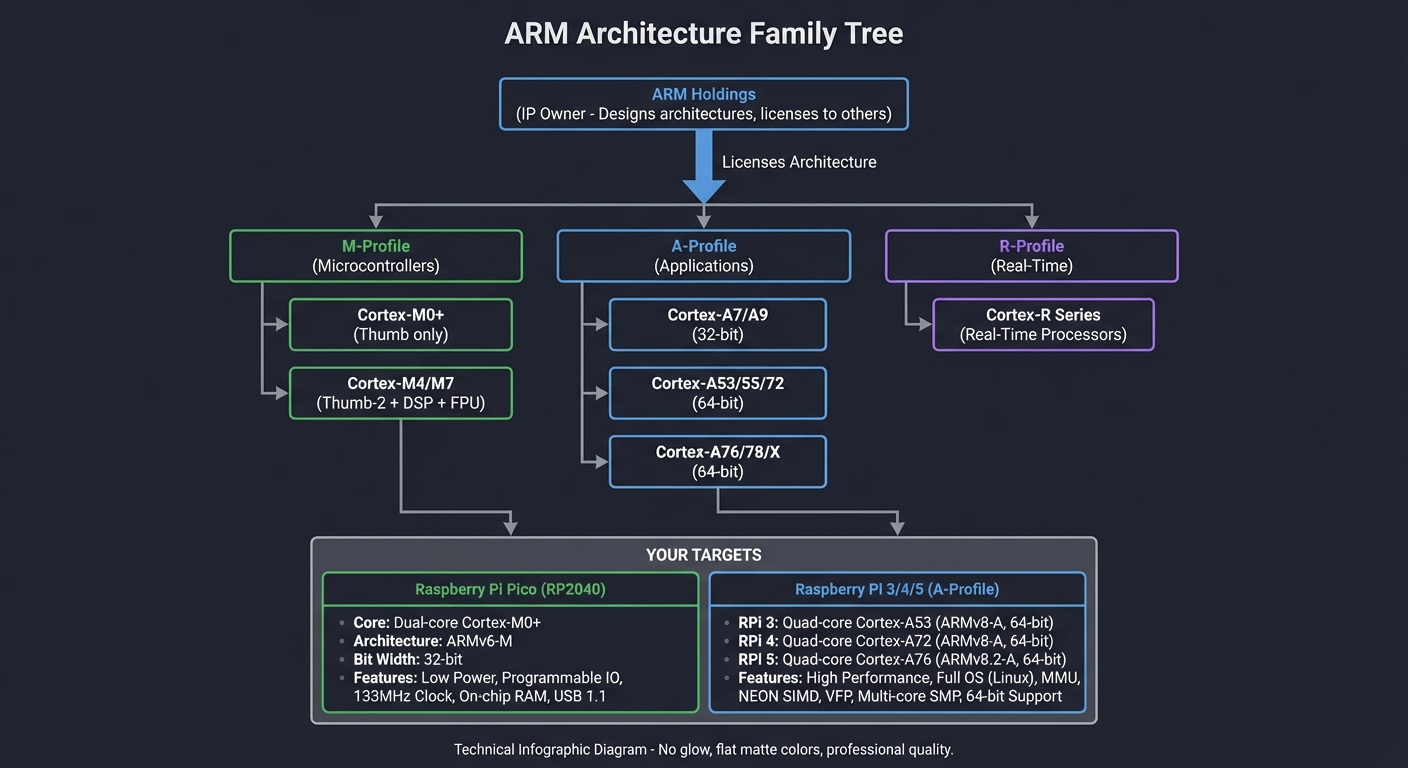
Fundamentals ARM is a family of architectures organized into profiles optimized for different constraints. The A-profile targets application processors that run rich OSes (phones, laptops, servers), the M-profile targets microcontrollers with tight power and memory budgets, and the R-profile targets deterministic real-time systems. citeturn0search0turn0search1turn0search2 Each profile implies a different set of instructions, privilege models, and system features. Within a profile, ARM defines execution states (such as AArch64 or AArch32) that determine register width, instruction encoding, and address space. AArch64 is the 64-bit execution state introduced in ARMv8-A, while AArch32 is the 32-bit state; M-profile uses Thumb encodings for compact code density and simpler decode logic. citeturn0search2 This is why “ARM assembly” is not a single language: the same mnemonic can encode differently, or even be invalid, depending on profile and state.
Deep Dive The profile split is the most important high-level idea in ARM. A-profile cores are built to host complex operating systems with virtual memory, multi-core scheduling, and high performance. That means features like exception levels, MMUs, and richer instruction sets matter. In contrast, M-profile focuses on minimal latency, low power, and deterministic behavior: it strips away many features to reduce silicon cost and simplify real-time response. R-profile sits in-between: it retains more predictability than A-profile but includes stronger real-time guarantees than M-profile. citeturn0search0turn0search1 When you choose to write assembly, you’re implicitly choosing a profile, and that choice changes everything from the boot flow to the toolchain arguments you use.
Execution states deepen the split. In ARMv8-A, AArch64 brings a new 64-bit register file and 32-bit fixed-length instruction encoding (A64). AArch32 keeps the 32-bit model (A32/T32). This means that for A-profile hardware, your code must declare its intended execution state; otherwise, even valid mnemonics may assemble into the wrong encoding or fail. citeturn0search2 M-profile, by contrast, uses Thumb encodings by design, favoring compact instructions and simpler decode paths. These constraints are not academic. They drive register availability, calling convention differences, and even the structure of your interrupt handlers. If you write code that assumes AArch64 but run on Cortex-M, the encoding and semantics are incompatible.
Another subtle but critical effect of profile and state is the system-level context. A-profile expects multiple privilege levels and potentially a hypervisor. M-profile’s exception model is simpler, its vector table is fixed and immediate, and it typically boots directly into a single firmware image. R-profile targets systems where real-time guarantees trump throughput; this affects interrupt priority, memory latency assumptions, and peripheral access patterns. Understanding profile choice lets you reason about why an instruction exists, why a particular addressing mode is missing, and why certain system registers are visible or hidden.
Finally, architecture profiles determine the ecosystem around your work. A-profile benefits from abundant tooling, standardized ABIs, and OS integration, while M-profile leans on vendor SDKs, board-specific memory maps, and smaller toolchains. This guide intentionally spans both because many real-world systems combine them: a Linux-capable application processor for high-level features and a microcontroller for deterministic control. Once you see that split, you can design experiments and projects that map to the right target without confusion.
How this fits on projects
- Shapes target selection in P01 (Toolchain Pipeline Explorer) and P07 (Exception Level Lab).
- Determines encoding assumptions in P03 (Thumb Encoder/Decoder).
Definitions & key terms
- Profile: A family of ARM features optimized for a market segment (A/M/R). citeturn0search0turn0search1turn0search2
- Execution state: The architectural mode (AArch64, AArch32, Thumb) that defines register width and instruction encoding. citeturn0search2
- AArch64: 64-bit execution state introduced in ARMv8-A.
- AArch32: 32-bit execution state in ARMv8-A.
- Thumb: Compact instruction encoding used by M-profile.
Mental model diagram
ARM Architecture Evolution:
━━━━━━━━━━━━━━━━━━━━━━━━━━━━━━━━━━━━━━━━━━━━━━━━━━━━━━━━━━━━━━━━━━━━━━━━━━━━━

                              ┌─────────────────────────────────────────────┐
                              │            ARM Holdings (IP owner)           │
                              │   Designs architectures, licenses to others  │
                              └─────────────────────┬───────────────────────┘
                                                    │
           ┌────────────────────────────────────────┼────────────────────────────┐
           │                                        │                            │
           ▼                                        ▼                            ▼
    ┌──────────────┐                    ┌────────────────┐              ┌────────────────┐
    │   M-Profile  │                    │    A-Profile   │              │   R-Profile    │
    │ Microcontrollers                  │  Applications  │              │   Real-Time    │
    │ (Embedded)   │                    │ (Phones, PCs)  │              │   (Automotive) │
    └──────────────┘                    └────────────────┘              └────────────────┘
           │                                        │
    ┌──────┴──────┐                    ┌────────────┼────────────┐
    │             │                    │            │            │
    ▼             ▼                    ▼            ▼            ▼
 ┌───────┐   ┌────────┐          ┌─────────┐  ┌─────────┐  ┌─────────┐
 │Cortex │   │Cortex  │          │Cortex-A7│  │Cortex-A │  │Cortex-A │
 │ -M0+  │   │-M4/M7  │          │Cortex-A9│  │53/55/72 │  │76/78/X  │
 │       │   │        │          │(32-bit) │  │(64-bit) │  │(64-bit) │
 └───────┘   └────────┘          └─────────┘  └─────────┘  └─────────┘
     │            │                   │            │            │
     │            │                   │            │            │
  Thumb       Thumb-2              ARM32      AArch64      AArch64
  only        + DSP               + Thumb    + NEON       + SVE2
                + FPU

┌──────────────────────────────────────────────────────────────────────────────┐
│ YOUR TARGETS:                                                                 │
│                                                                               │
│ Raspberry Pi Pico (RP2040)     Raspberry Pi 3/4/5                            │
│ ├─ Dual Cortex-M0+ cores       ├─ Cortex-A53/A72/A76 cores                   │
│ ├─ ARMv6-M architecture        ├─ ARMv8-A architecture (AArch64)             │
│ ├─ Thumb instruction set       ├─ A64 instruction set                        │
│ ├─ 16 registers (r0-r15)       ├─ 31 registers (x0-x30)                      │
│ ├─ 133 MHz max clock           ├─ 1.5-2.4 GHz clock                          │
│ └─ 264 KB RAM, no OS           └─ 1-8 GB RAM, Linux capable                  │
└──────────────────────────────────────────────────────────────────────────────┘
How it works (step-by-step, with invariants and failure modes)
- Choose the target profile (A/M/R) based on system constraints and OS expectations.
- Select execution state (AArch64, AArch32, Thumb) based on ISA and toolchain output.
- Assemble and link with profile/state-specific flags; encoding mismatches yield invalid opcodes.
- Boot into the expected privilege level; if the firmware expects EL2 and you start at EL1, early setup fails.
- Validate on target or emulator; incorrect profile assumptions manifest as illegal instruction faults or boot hangs.
Minimal concrete example (pseudo-assembly, not runnable)
Select Target = {Profile: M, State: Thumb}
Assemble([LOAD R0, [ADDR]], Target)
If Target != CPU_State → Fault: Illegal Instruction
Common misconceptions
- “ARM assembly is one language” → It is a family with profile/state splits.
- “Thumb is only a compact mode” → It also shapes register access and available instructions.
- “AArch64 is just ARM32 with bigger registers” → It changes the register file and encoding model.
Check-your-understanding questions
- Why can Cortex-M code not run on a Cortex-A core without translation?
- What is the difference between AArch64 and AArch32?
- How does the profile choice affect your toolchain flags?
Check-your-understanding answers
- Cortex-M uses the M-profile with Thumb encodings and a different system model; Cortex-A expects A-profile with AArch64/AArch32 states.
- AArch64 is a 64-bit execution state with a new register file and A64 encoding; AArch32 is 32-bit with different encodings. citeturn0search2
- The assembler and linker must emit instructions for the correct ISA and object format; mismatches produce illegal opcodes or link errors.
Real-world applications
- Microcontroller firmware (M-profile) in sensors, robotics, and embedded control. citeturn0search0
- Application processors (A-profile) in mobile, desktop, and servers. citeturn0search2
Where you’ll apply it
- P01 Toolchain Pipeline Explorer
- P03 Thumb Instruction Encoder/Decoder
- P07 AArch64 Exception Level Lab
References
- Arm M-profile overview. citeturn0search0
- Arm R-profile overview. citeturn0search1
- Arm A-profile overview and execution states. citeturn0search2
Key insights Your “ARM assembly” only makes sense once you name the profile and execution state.
Summary Profiles and execution states are the root of every other difference in ARM assembly. When you get this right, the rest of the system becomes predictable.
Homework/Exercises to practice the concept
- Pick two devices (one microcontroller, one phone) and identify their ARM profile and execution state.
- Write a one-paragraph explanation of why Thumb exists.
Solutions to the homework/exercises
- Example: RP2040 is M-profile with Thumb; a modern smartphone SoC is A-profile with AArch64.
- Thumb improves code density and decoder simplicity, which is crucial for small embedded systems.
Concept 2: Registers, Stack, and Calling Conventions
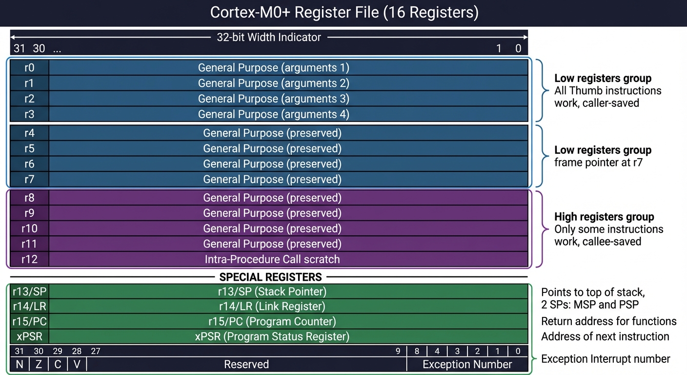
Fundamentals Registers are the CPU’s fastest storage and form the working set for computation. ARM profiles differ in register count and special-purpose roles, but all share the idea that function calls require a contract: how arguments and return values are passed, which registers must be preserved, and how the stack is organized. The procedure call standard defines this contract so independently compiled code can interoperate. citeturn3search7 In Cortex-M, the register file is small and heavily constrained by Thumb encoding, whereas AArch64 offers 31 general-purpose registers and a distinct separation between 64-bit (X) and 32-bit (W) views. citeturn2search0 The stack pointer and link register govern call/return flow, and misusing them corrupts control flow even if individual instructions look correct.
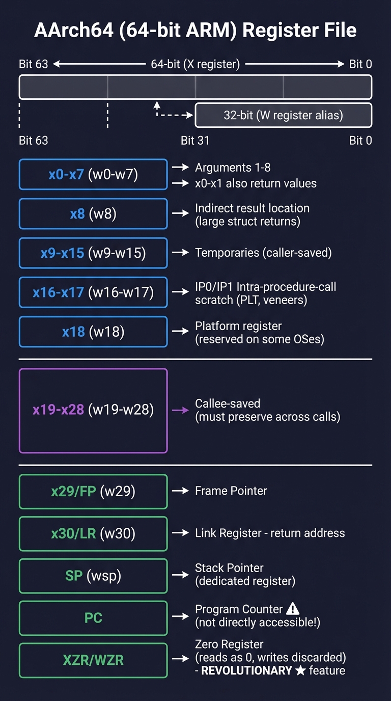
Deep Dive The register file is the interface between the ISA and your mental model. On Cortex-M0+, you have 16 architectural registers (r0–r15), with r13 as the stack pointer, r14 as the link register (return address), and r15 as the program counter. Thumb encodings make low registers (r0–r7) more convenient, and this shapes how you allocate values and temporaries. On AArch64, the register file expands to 31 general-purpose registers (x0–x30), plus a dedicated SP. The lower 32-bit view (w0–w30) is an alias, not separate storage. citeturn2search0 This abundance reduces register pressure but increases the importance of ABI rules to maintain interoperability.
Calling conventions are not optional. They define which registers hold arguments, which registers are caller-saved or callee-saved, and how the stack is aligned. The AAPCS64 procedure call standard formalizes this for AArch64, and the same principle applies to Cortex-M via EABI conventions. citeturn3search7 If a function trashes a callee-saved register or returns with an unbalanced stack pointer, the next return will jump to a garbage address. The stack is not merely a place to store locals: it is a control-flow structure with strict invariants. Typical invariants include: the stack pointer must remain aligned to a fixed boundary at call boundaries, return addresses must be preserved (often via LR), and exception frames must be compatible with hardware expectations.
The difference between M-profile and A-profile also affects how you reason about stack frames and interrupts. Cortex-M pushes a standard register frame on interrupt entry and uses special EXC_RETURN values to restore state. AArch64 exceptions are higher-level and interact with exception levels (EL0–EL3). This means the calling convention is entangled with the exception model: you must ensure that the register context saved by an ISR matches what the hardware expects, and that your handler preserves the right registers. Even if you never write an ISR, debugging requires you to recognize how the stack frame was laid out and which registers are live at a given moment.
Finally, registers are a performance and correctness story. Keeping hot values in registers avoids memory latency, but retaining too many values across calls increases spill overhead and complexity. The ABI is a compromise: caller-saved registers allow fast leaf functions to avoid stack usage, while callee-saved registers allow values to persist across deeper calls. Understanding this trade-off is what turns disassembly from a wall of text into a readable narrative.
How this fits on projects
- Central to P02 (Register and Stack Visualizer) and P08 (Calling Convention Audit).
Definitions & key terms
- Register file: The set of architectural registers visible to instructions.
- Caller-saved: Registers a caller must preserve if it needs their values after a call.
- Callee-saved: Registers a callee must preserve across the call. citeturn3search7
- Stack frame: A structured region on the stack holding locals and saved state.
- Procedure call standard: ABI rules for passing arguments and preserving registers. citeturn3search7
Mental model diagram
Cortex-M0+ Register File:
━━━━━━━━━━━━━━━━━━━━━━━━━━━━━━━━━━━━━━━━━━━━━━━━━━━━━━━━━━━━━━━━━━━━━━━━

                    32 bits wide
              ◀──────────────────▶

    ┌───────────────────────────────┐
r0  │  General Purpose (argument 1) │  ─┐
    ├───────────────────────────────┤   │
r1  │  General Purpose (argument 2) │   │  Low registers:
    ├───────────────────────────────┤   │  - All Thumb instructions work
r2  │  General Purpose (argument 3) │   │  - Used for function arguments
    ├───────────────────────────────┤   │    and return values
r3  │  General Purpose (argument 4) │   │  - Caller-saved (scratch)
    ├───────────────────────────────┤   │
r4  │  General Purpose (preserved)  │   │
    ├───────────────────────────────┤   │
r5  │  General Purpose (preserved)  │   │
    ├───────────────────────────────┤   │
r6  │  General Purpose (preserved)  │   │
    ├───────────────────────────────┤   │
r7  │  General Purpose (frame ptr)  │  ─┘
    ├───────────────────────────────┤
r8  │  General Purpose (preserved)  │  ─┐  High registers:
    ├───────────────────────────────┤   │  - Only some instructions work
r9  │  General Purpose (preserved)  │   │  - Must move to low reg for
    ├───────────────────────────────┤   │    most operations
r10 │  General Purpose (preserved)  │   │  - Callee-saved
    ├───────────────────────────────┤   │
r11 │  General Purpose (preserved)  │   │
    ├───────────────────────────────┤   │
r12 │  Intra-Procedure Call scratch │  ─┘
    ├═══════════════════════════════┤  ────  SPECIAL REGISTERS  ────
r13 │  Stack Pointer (SP)           │  Points to top of stack
    ├───────────────────────────────┤  (actually 2 SPs: MSP and PSP)
r14 │  Link Register (LR)           │  Return address for functions
    ├───────────────────────────────┤
r15 │  Program Counter (PC)         │  Address of next instruction
    └───────────────────────────────┘

    ┌───────────────────────────────┐
xPSR│ N│Z│C│V│ ... │ Exception #   │  Program Status Register:
    └─┬─┴─┴─┴─────────────────────┴─┘  N = Negative, Z = Zero
      │                                 C = Carry, V = Overflow
      └─ Condition flags set by
         arithmetic operations

IMPORTANT: Cortex-M0+ has NO program counter-relative addressing for
data. You MUST use literal pools or calculate addresses manually!
AArch64 Register File:
━━━━━━━━━━━━━━━━━━━━━━━━━━━━━━━━━━━━━━━━━━━━━━━━━━━━━━━━━━━━━━━━━━━━━━━━

             64 bits wide (X registers)
      ◀──────────────────────────────────────────▶
      │    32 bits (W register alias)            │
      │                    ◀─────────────────────┤

    ┌───────────────────────────────────────────────────────────────┐
x0  │  Argument 1 / Return value                                    │  w0
    ├───────────────────────────────────────────────────────────────┤
x1  │  Argument 2 / Return value (for 128-bit returns)              │  w1
    ├───────────────────────────────────────────────────────────────┤
x2  │  Argument 3                                                   │  w2
    ├───────────────────────────────────────────────────────────────┤
...                        ...
    ├───────────────────────────────────────────────────────────────┤
x7  │  Argument 8                                                   │  w7
    ├───────────────────────────────────────────────────────────────┤
x8  │  Indirect result location (for large struct returns)         │  w8
    ├───────────────────────────────────────────────────────────────┤
x9  │  Temporary / Caller-saved                                     │  w9
    ├───────────────────────────────────────────────────────────────┤
... │  x9-x15: Temporaries (caller-saved)                           │
    ├───────────────────────────────────────────────────────────────┤
x16 │  IP0 - Intra-procedure-call scratch (PLT, veneers)           │  w16
    ├───────────────────────────────────────────────────────────────┤
x17 │  IP1 - Intra-procedure-call scratch                          │  w17
    ├───────────────────────────────────────────────────────────────┤
x18 │  Platform register (reserved on some OSes)                    │  w18
    ├───────────────────────────────────────────────────────────────┤
x19 │  Callee-saved (must preserve across calls)                    │  w19
    ├───────────────────────────────────────────────────────────────┤
... │  x19-x28: Callee-saved                                        │
    ├═══════════════════════════════════════════════════════════════┤
x29 │  Frame Pointer (FP)                                           │  w29
    ├───────────────────────────────────────────────────────────────┤
x30 │  Link Register (LR) - return address                          │  w30
    ├───────────────────────────────────────────────────────────────┤
SP  │  Stack Pointer (not a GPR, dedicated register)                │  wsp
    ├───────────────────────────────────────────────────────────────┤
PC  │  Program Counter (not directly accessible like ARM32!)        │
    └───────────────────────────────────────────────────────────────┘

    ┌───────────────────────────────────────────────────────────────┐
XZR │  Zero Register (reads as 0, writes discarded)                 │  wzr
    └───────────────────────────────────────────────────────────────┘
      ^ This is REVOLUTIONARY - no wasted instruction to clear!


SIMD/Floating-Point Registers (32 × 128-bit):
━━━━━━━━━━━━━━━━━━━━━━━━━━━━━━━━━━━━━━━━━━━━━━━━━━━━━━━━━━━━━━━━━━━━━━━━

    ┌───────────────────────────────────────────────────────────────┐
v0  │  B0│B1│B2│...│B15│  ← 16 bytes = 128 bits (Q0/V0)            │
    │  H0│H1│...│H7    │  ← 8 halfwords                             │
    │  S0│S1│S2│S3     │  ← 4 singles (float)                       │
    │  D0│D1           │  ← 2 doubles                               │
    └───────────────────────────────────────────────────────────────┘

    Used for: floating-point, SIMD (NEON), and crypto operations


Key Differences from ARM32:
━━━━━━━━━━━━━━━━━━━━━━━━━━━━━━━━━━━━━━━━━━━━━━━━━━━━━━━━━━━━━━━━━━━━━━━━
  • 31 GPRs (vs 16) → Less register pressure, fewer spills
  • PC not directly readable/writable → Use ADR/ADRP for addresses
  • Zero register (xzr/wzr) → MOV x0, xzr instead of MOV r0, #0
  • No conditional execution → Use CSEL, CSINC instead
  • 64-bit addresses → Can address all of RAM directly
  • All instructions 32-bit → No 16-bit Thumb encoding
How it works (step-by-step, with invariants and failure modes)
- Arguments are placed in registers according to the ABI contract. citeturn3search7
- Callee preserves its required registers and sets up a stack frame if needed.
- Return value is placed in the agreed register(s) before restoring SP and LR.
- Failure mode: If SP alignment is violated or callee-saved registers are clobbered, returns jump to wrong addresses or data corrupts silently.
Minimal concrete example (pseudo-assembly, not runnable)
CALL f(a,b):
  ARG0 <- a
  ARG1 <- b
  LR   <- return_address
  SP   <- SP - frame_size
  ...
  return: restore SP, jump LR
Common misconceptions
- “More registers always mean simpler code” → ABI rules still constrain usage.
- “Stack is just a data structure” → It also encodes control flow.
Check-your-understanding questions
- Why does the ABI require callee-saved registers?
- What happens if a function returns without restoring SP?
- Why does AArch64 expose 31 GPRs instead of 16?
Check-your-understanding answers
- It lets callers rely on certain registers surviving across calls, enabling composition. citeturn3search7
- The return address is read from the wrong stack location, leading to a crash or silent corruption.
- AArch64’s design prioritizes performance and reduced spills; the larger register file supports that. citeturn2search0
Real-world applications
- Disassembly analysis for security or performance auditing.
- Interfacing assembly routines with C libraries. citeturn3search7
Where you’ll apply it
- P02 Register and Stack Visualizer
- P08 Calling Convention Audit
References
- AArch64 register model overview. citeturn2search0
- AAPCS64 procedure call standard. citeturn3search7
Key insights Calling conventions are the glue that makes low-level code composable.
Summary Registers and the stack are not independent; they form a contract that every function must obey.
Homework/Exercises to practice the concept
- Draw a stack frame for a function that calls two helpers and uses three local variables.
- Identify which registers you would preserve in a callee according to a generic ABI.
Solutions to the homework/exercises
- The frame must allocate locals, save the return address, and preserve any callee-saved registers used.
- Preserve registers designated as callee-saved in the ABI; all others are caller-saved.
Concept 3: Instruction Encoding and Addressing Modes
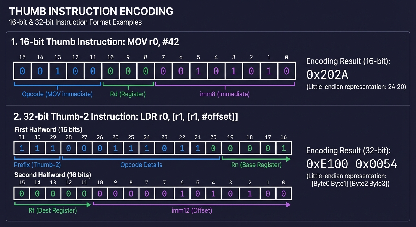
Fundamentals Every assembly instruction is encoded into bits. Encoding determines which registers and immediates are accessible, how large constants can be, and which addressing modes are legal. Thumb encodings prioritize compactness and energy efficiency for microcontrollers, while AArch64 uses fixed 32-bit instruction widths to simplify decode and improve pipeline predictability. citeturn0search2 Understanding encoding explains why some instructions are missing or require multi-instruction sequences and why certain address calculations must be split into steps.
Deep Dive
Instruction encoding is the “physics” of assembly. A mnemonic like MOV is a human label for a specific bit pattern; if that pattern cannot fit your operands, the assembler will either refuse or emit a different instruction sequence. Thumb uses a mix of 16-bit and 32-bit encodings (Thumb-2), which means register and immediate fields are often smaller. This is why Cortex-M uses a small set of low registers more naturally and why large constants must be loaded via literal pools or multi-step sequences. AArch64, in contrast, uses 32-bit instructions exclusively, providing more predictable decoding and a richer register space. citeturn0search2 The trade-off is code density versus decode simplicity.
Addressing modes compound encoding constraints. Load/store architectures like ARM separate arithmetic from memory access: you compute addresses in registers, then load or store. But the address computation itself is limited by encoding fields. For example, immediate offsets might be limited to a certain bit width or require alignment. When you understand the bit fields, you can predict when the assembler will need to generate extra instructions, which in turn affects performance and size. This is especially important in microcontrollers where code size is constrained and instruction fetches may come from slow flash.
Encoding also interacts with endianness and instruction alignment. Many ARM cores require instructions to be aligned to 2 or 4 bytes depending on the ISA. Misalignment results in faults or unintended behavior. The assembler handles alignment for you, but if you build a binary layout manually (for example in a boot image), you must respect alignment rules to avoid hard-to-debug startup failures. This is why toolchain awareness is an essential complement to ISA knowledge.
Finally, encoding shapes the patterns you see in disassembly. A sequence of machine code bytes can decode to different instructions depending on execution state. This is a common pitfall in reverse engineering: decoding AArch64 bytes as Thumb or ARM32 yields nonsense. Knowing the encoding class prevents misinterpretation and helps you verify that your build pipeline is producing the ISA you intended.
How this fits on projects
- Core to P03 (Thumb Instruction Encoder/Decoder) and P01 (Toolchain Pipeline Explorer).
Definitions & key terms
- Encoding: Bit-level representation of an instruction.
- Addressing mode: How an instruction specifies the location of its operands.
- Thumb/Thumb-2: Compact ARM instruction encodings for M-profile.
- A64: 32-bit fixed-length instruction encoding for AArch64. citeturn0search2
Mental model diagram
Thumb Instruction Encoding Examples:
━━━━━━━━━━━━━━━━━━━━━━━━━━━━━━━━━━━━━━━━━━━━━━━━━━━━━━━━━━━━━━━━━━━━━━━━

16-bit Thumb instruction: MOV r0, #42
┌──┬──┬──┬──┬──┬──┬──┬──┬──┬──┬──┬──┬──┬──┬──┬──┐
│ 0│ 0│ 1│ 0│ 0│ Rd  │     imm8 (immediate)    │
│ 0│ 0│ 1│ 0│ 0│0│0│0│ 0│ 0│ 1│ 0│ 1│ 0│ 1│ 0│
└──┴──┴──┴──┴──┴──┴──┴──┴──┴──┴──┴──┴──┴──┴──┴──┘
              │r0 │         42 = 0x2A
              │   │
              ▼   ▼
          Encodes to: 0x202A (little-endian: 2A 20)


32-bit Thumb-2 instruction: LDR r0, [r1, #offset]  (when offset > 31)
┌──────────────────────────────────────────────────────────────────┐
│ First halfword (16 bits)  │  Second halfword (16 bits)           │
│   encoding prefix + Rn    │     Rt + imm12 offset                │
└──────────────────────────────────────────────────────────────────┘


Common Thumb Instructions You'll Use:
━━━━━━━━━━━━━━━━━━━━━━━━━━━━━━━━━━━━━━━━━━━━━━━━━━━━━━━━━━━━━━━━━━━━━━━━

Data Movement:
  MOV  Rd, #imm8        Move 8-bit immediate to register
  MOV  Rd, Rm           Move register to register
  LDR  Rt, [Rn, #off]   Load word from memory
  STR  Rt, [Rn, #off]   Store word to memory
  PUSH {reglist}        Push registers to stack
  POP  {reglist}        Pop registers from stack

Arithmetic:
  ADD  Rd, Rn, #imm3    Add 3-bit immediate
  ADD  Rd, #imm8        Add 8-bit immediate to Rd
  SUB  Rd, Rn, #imm3    Subtract 3-bit immediate
  SUBS Rd, Rn, Rm       Subtract with flags update

Logic:
  AND  Rd, Rm           Bitwise AND
  ORR  Rd, Rm           Bitwise OR
  EOR  Rd, Rm           Bitwise XOR (exclusive OR)
  LSL  Rd, Rm, #imm5    Logical shift left
  LSR  Rd, Rm, #imm5    Logical shift right

Control Flow:
  B    label            Unconditional branch
  BEQ  label            Branch if equal (Z=1)
  BNE  label            Branch if not equal (Z=0)
  BL   function         Branch with link (function call)
  BX   Rm               Branch to address in register
  BLX  Rm               Branch with link to address in register


LIMITATION: Cortex-M0+ is MISSING many instructions!
━━━━━━━━━━━━━━━━━━━━━━━━━━━━━━━━━━━━━━━━━━━━━━━━━━━━━━━━━━━━━━━━━━━━━━━━
✗ No hardware divide (UDIV, SDIV)     → Must use software division
✗ No bit-field instructions (BFI)     → Must use shift/mask sequences
✗ No conditional execution (IT block) → Must use branches
✗ Limited addressing modes            → Can't do [Rn, Rm, LSL #2]
✗ No saturation arithmetic            → Must check overflow manually
How it works (step-by-step, with invariants and failure modes)
- The assembler maps mnemonics to encoding templates for the target ISA.
- Register and immediate fields are packed into fixed bit positions.
- If a value doesn’t fit, the assembler emits a sequence or errors out.
- Failure mode: decoding with the wrong ISA yields invalid instructions or faults.
Minimal concrete example (pseudo, not runnable)
ENCODE(op=ADD, rd=R0, rn=R1, imm=5)
→ [opcode bits][rd bits][rn bits][imm bits]
Common misconceptions
- “Assembler will always accept my operands” → Encoding limits still apply.
- “Instruction length doesn’t matter” → It affects alignment and memory layout.
Check-your-understanding questions
- Why does Thumb use shorter encodings than AArch64?
- What happens if an immediate is too large for its field?
- Why can decoding with the wrong execution state break disassembly?
Check-your-understanding answers
- Thumb optimizes for code density and decoder simplicity in M-profile contexts. citeturn0search2
- The assembler emits a sequence or reports an error because it cannot fit the value.
- The same bytes map to different instruction sets depending on state, so decoding mismatches yield nonsense.
Real-world applications
- Building encoders/decoders for tooling and reverse engineering.
- Size-sensitive firmware builds for microcontrollers.
Where you’ll apply it
- P03 Thumb Instruction Encoder/Decoder
- P01 Toolchain Pipeline Explorer
References
- Arm A-profile overview (AArch64, instruction model). citeturn0search2
Key insights Encoding constraints explain most “mysterious” assembler errors.
Summary Instruction encodings are the boundary between human mnemonics and machine reality; mastering them unlocks predictability.
Homework/Exercises to practice the concept
- Choose a Thumb instruction and manually identify which bits encode the register fields.
- Explain why a large constant may require multiple instructions.
Solutions to the homework/exercises
- The register fields are fixed bit slices in the instruction encoding; their size limits which registers are directly addressable.
- If the immediate field is too small, the assembler must build the constant through multiple steps.
Concept 4: Memory Maps, MMIO, and Memory Ordering
Fundamentals ARM systems expose peripherals through memory-mapped I/O (MMIO): reading or writing specific addresses triggers hardware behavior rather than normal memory access. This is central to microcontrollers and still vital on A-profile SoCs. The memory map defines which address ranges are RAM, flash, peripherals, and internal control regions. Memory ordering adds another layer: modern CPUs can reorder memory accesses for performance, so barriers (DMB/DSB/ISB) are required to guarantee visibility and ordering to devices or other cores. citeturn3search3 Understanding MMIO and ordering is the key to controlling hardware reliably.
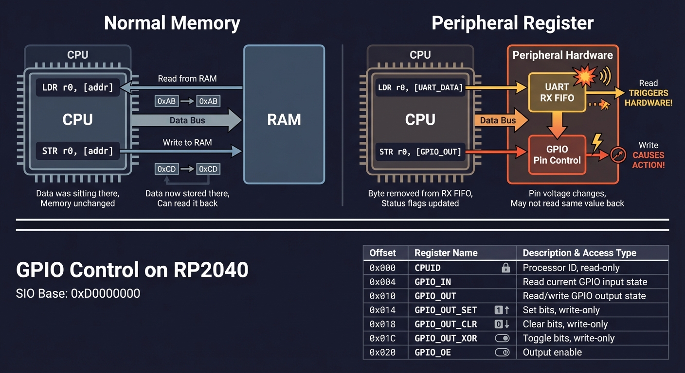
Deep Dive A memory map is a contract between the CPU and the SoC. Addresses are not abstract: they correspond to real hardware blocks. In Cortex-M systems, large fixed ranges map to flash, SRAM, peripherals, and internal control registers. These ranges determine what happens when you load or store. For example, a store to a GPIO register flips a pin; a load from a UART data register consumes a byte from a FIFO. MMIO behaves differently from RAM: it is often non-cacheable, may have side effects on read, and is frequently write-only or read-only. When you treat it like ordinary memory, bugs emerge: stale values, missing updates, or unintended state changes.
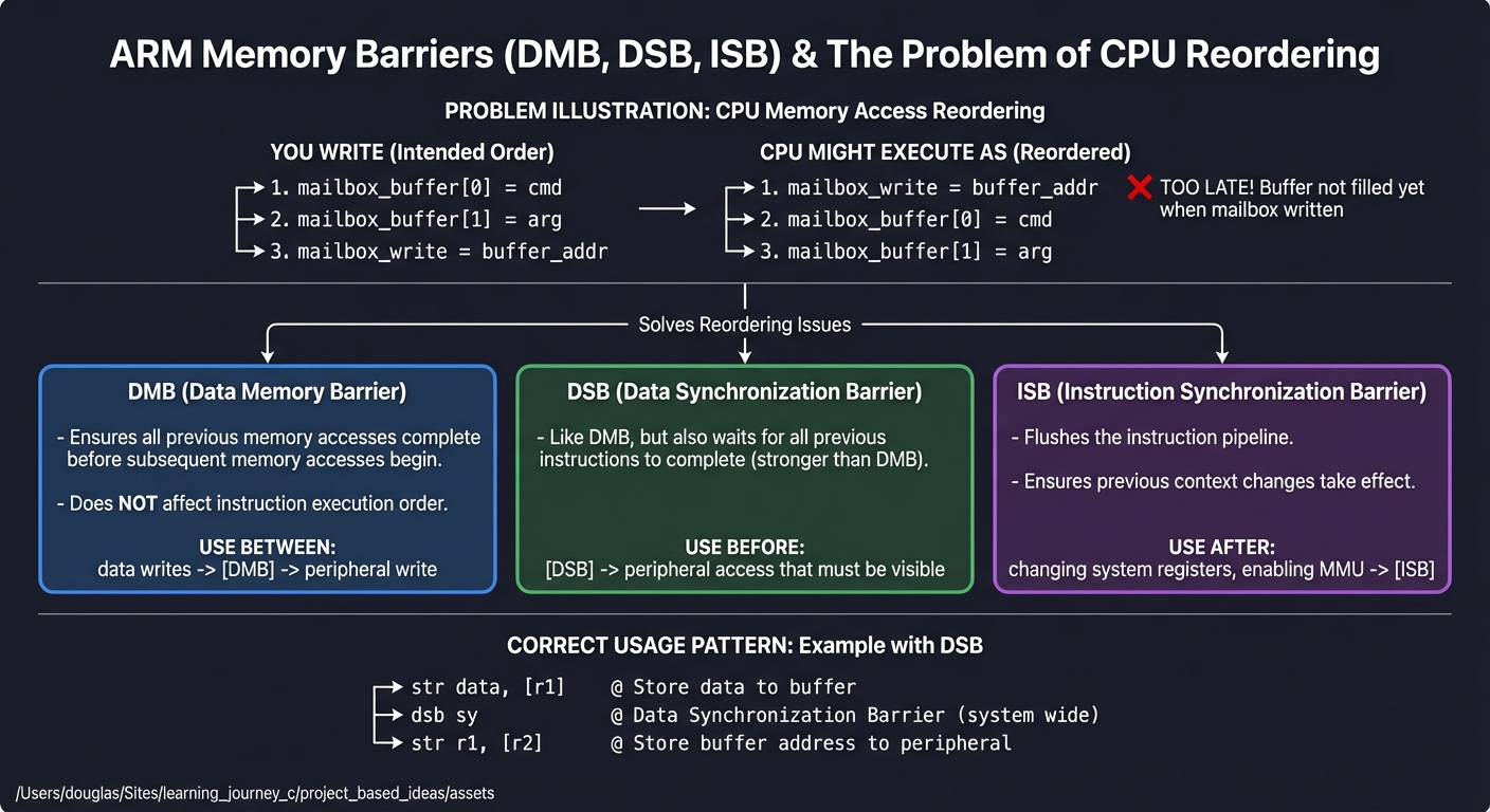
Memory ordering complicates this further. ARM cores, like most modern CPUs, can reorder memory operations to improve performance. This is invisible in single-threaded logic but catastrophic for devices and multi-core coordination. If you write a command buffer to memory and then write a “doorbell” MMIO register that tells the device to consume it, the device might see the doorbell first unless you insert a barrier. ARM provides barrier instructions—DMB, DSB, ISB—each with distinct strength. DMB ensures prior memory accesses are observed before subsequent ones; DSB additionally waits for completion; ISB flushes the instruction pipeline to make control-register changes visible. citeturn3search3 These are not optional: they are the difference between “mostly works” and “always correct.”
On microcontrollers, you may not have caches or complex reorder buffers, but the bus fabric and peripheral interactions still require ordering. On A-profile systems with caches, speculation, and out-of-order execution, the need is even greater. DMA engines read and write memory independently of the CPU; if you don’t synchronize caches or enforce ordering, the DMA sees stale or partial data. This is why firmware often combines barriers with explicit cache maintenance. The principle is simple: your mental model must include the device, the bus, and the CPU pipeline, not just the instruction sequence.
MMIO access patterns also introduce concurrency hazards. Read-modify-write sequences can race with interrupts or other cores. Hardware often provides SET/CLEAR registers specifically to avoid these races by allowing atomic bit operations. If you ignore these and perform a naive read-modify-write, you can silently clear unrelated bits. The safest approach is to understand the register semantics and use the atomic registers provided. That is not assembly-specific, but assembly exposes the pattern directly and makes it obvious.
How this fits on projects
- Core to P04 (Memory Map & MMIO Field Notebook) and P09 (Memory Ordering Litmus Tests).
Definitions & key terms
- Memory map: The assignment of address ranges to RAM, flash, and peripherals.
- MMIO: Memory addresses that control hardware rather than store data.
- DMB/DSB/ISB: Memory barrier instructions for ordering and visibility. citeturn3search3
Mental model diagram
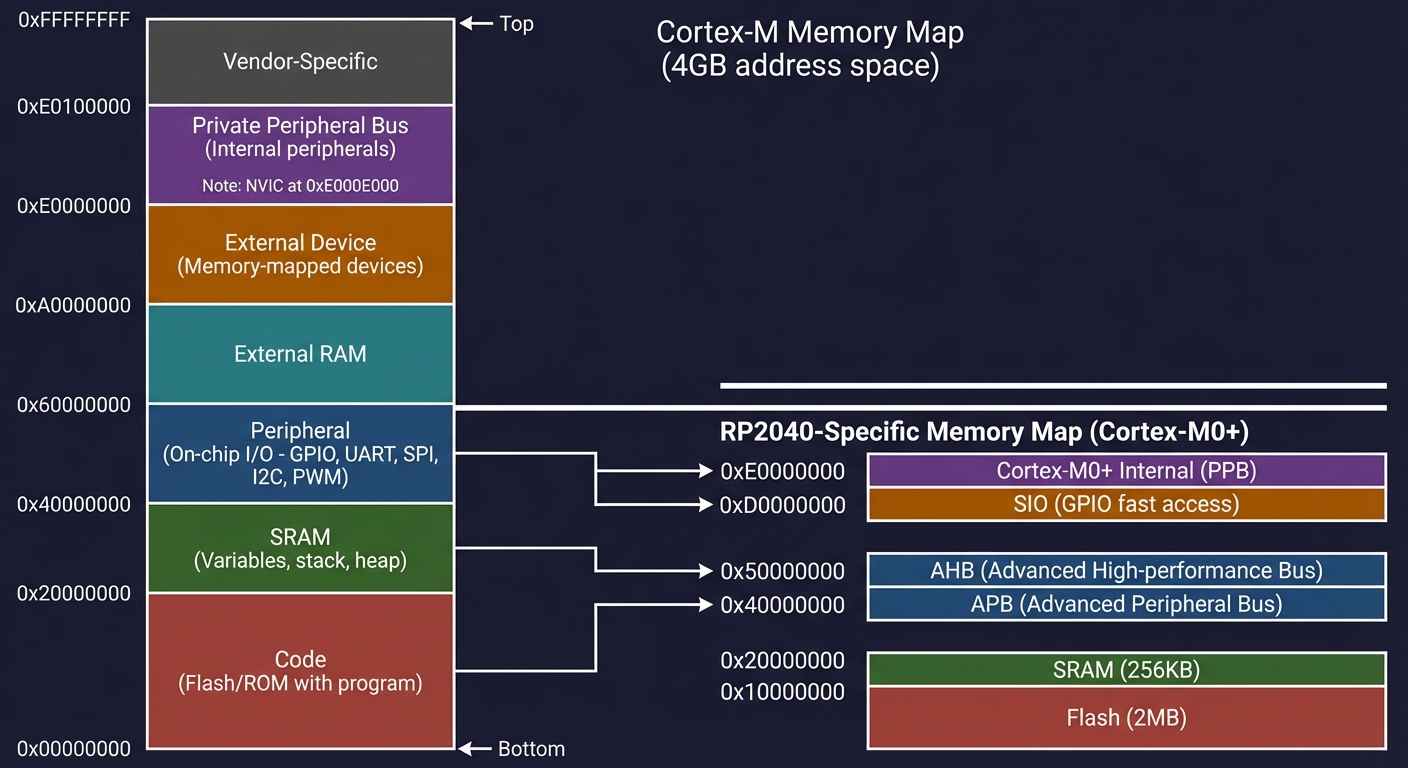
Cortex-M Memory Map (4GB address space):
━━━━━━━━━━━━━━━━━━━━━━━━━━━━━━━━━━━━━━━━━━━━━━━━━━━━━━━━━━━━━━━━━━━━━━━━

    0xFFFFFFFF ┌─────────────────────────────────────────┐
               │         Vendor-Specific                 │
    0xE0100000 ├─────────────────────────────────────────┤
               │         Private Peripheral Bus          │  ← NVIC lives here
               │         (Internal peripherals)          │    at 0xE000E000
    0xE0000000 ├─────────────────────────────────────────┤
               │                                         │
               │         External Device                 │  ← Memory-mapped
               │         (Peripherals, etc.)             │    devices
               │                                         │
    0xA0000000 ├─────────────────────────────────────────┤
               │                                         │
               │         External RAM                    │
               │                                         │
    0x60000000 ├─────────────────────────────────────────┤
               │                                         │
               │         Peripheral                      │  ← GPIO, UART, SPI,
               │         (On-chip I/O)                   │    I2C, PWM, etc.
               │                                         │
    0x40000000 ├─────────────────────────────────────────┤
               │                                         │
               │         SRAM                            │  ← Variables, stack,
               │         (On-chip RAM)                   │    heap
               │                                         │
    0x20000000 ├─────────────────────────────────────────┤
               │                                         │
               │         Code                            │  ← Flash/ROM with
               │         (Flash/ROM)                     │    your program
               │                                         │
    0x00000000 └─────────────────────────────────────────┘


RP2040-Specific Memory Map:
━━━━━━━━━━━━━━━━━━━━━━━━━━━━━━━━━━━━━━━━━━━━━━━━━━━━━━━━━━━━━━━━━━━━━━━━

    Address         │  Size      │  Contents
    ────────────────┼────────────┼─────────────────────────────────────
    0x10000000      │  2 MB      │  External Flash (XIP)
                    │            │  ↳ Your code runs from here
    ────────────────┼────────────┼─────────────────────────────────────
    0x20000000      │  256 KB    │  Main SRAM (4 banks × 64KB)
                    │            │  ↳ Variables, stack, heap
    0x20040000      │  4 KB      │  SRAM4 (for USB)
    0x20041000      │  4 KB      │  SRAM5 (for USB)
    ────────────────┼────────────┼─────────────────────────────────────
    0x40000000      │  -         │  APB Peripherals
                    │            │  ↳ UART, SPI, I2C, PWM...
    ────────────────┼────────────┼─────────────────────────────────────
    0x50000000      │  -         │  AHB-Lite Peripherals
                    │            │  ↳ DMA, USB, PIO...
    ────────────────┼────────────┼─────────────────────────────────────
    0xD0000000      │  -         │  SIO (Single-cycle I/O)
                    │            │  ↳ GPIO (fast access!)
    ────────────────┼────────────┼─────────────────────────────────────
    0xE0000000      │  -         │  Cortex-M0+ internal
                    │            │  ↳ NVIC, SysTick, Debug
Memory-Mapped I/O Concept:
━━━━━━━━━━━━━━━━━━━━━━━━━━━━━━━━━━━━━━━━━━━━━━━━━━━━━━━━━━━━━━━━━━━━━━━━

    Normal Memory:                  Peripheral Register:
    ──────────────                  ────────────────────
    LDR r0, [addr]                  LDR r0, [UART_DATA]
         │                               │
         ▼                               ▼
    Read from RAM                   Read TRIGGERS HARDWARE!
    Data was sitting there          Byte removed from RX FIFO
    Memory unchanged                Status flags updated

    STR r0, [addr]                  STR r0, [GPIO_OUT]
         │                               │
         ▼                               ▼
    Write to RAM                    Write CAUSES ACTION!
    Data now stored there           Pin voltage changes
    Can read it back                May not read same value back


Example: GPIO Control on RP2040:
━━━━━━━━━━━━━━━━━━━━━━━━━━━━━━━━━━━━━━━━━━━━━━━━━━━━━━━━━━━━━━━━━━━━━━━━

    SIO Base: 0xD0000000

    Offset  │ Register       │ Purpose
    ────────┼────────────────┼──────────────────────────────────
    0x000   │ CPUID          │ Processor ID (read-only)
    0x004   │ GPIO_IN        │ Read current GPIO input state
    0x010   │ GPIO_OUT       │ Read/write GPIO output state
    0x014   │ GPIO_OUT_SET   │ Set bits in GPIO_OUT (write-only)
    0x018   │ GPIO_OUT_CLR   │ Clear bits in GPIO_OUT (write-only)
    0x01C   │ GPIO_OUT_XOR   │ Toggle bits in GPIO_OUT (write-only)
    0x020   │ GPIO_OE        │ Output enable (1=output, 0=input)
    0x024   │ GPIO_OE_SET    │ Set bits in GPIO_OE
    0x028   │ GPIO_OE_CLR    │ Clear bits in GPIO_OE


    To turn ON GPIO25 (Pico's LED):
    ─────────────────────────────────────────────────────────────────

    LDR  r0, =0xD0000000     // SIO base address
    MOV  r1, #1
    LSL  r1, r1, #25         // r1 = 0x02000000 (bit 25)
    STR  r1, [r0, #0x024]    // GPIO_OE_SET: enable output
    STR  r1, [r0, #0x014]    // GPIO_OUT_SET: set high → LED ON!


    Why SET/CLR registers instead of just GPIO_OUT?
    ─────────────────────────────────────────────────────────────────

    Without SET/CLR (DANGEROUS):
    ┌────────────────────────────────────────────────────────────────┐
    │ LDR r1, [r0, #GPIO_OUT]   // Read current value                │
    │ ORR r1, r1, #(1<<25)      // Set bit 25                        │
    │ STR r1, [r0, #GPIO_OUT]   // Write back                        │
    │                                                                 │
    │ PROBLEM: If another core or interrupt modifies GPIO_OUT        │
    │ between the LDR and STR, those changes are LOST!               │
    │ This is a classic "read-modify-write race condition."          │
    └────────────────────────────────────────────────────────────────┘

    With SET/CLR (ATOMIC and SAFE):
    ┌────────────────────────────────────────────────────────────────┐
    │ MOV r1, #(1<<25)                                                │
    │ STR r1, [r0, #GPIO_OUT_SET]  // Hardware atomically sets bit   │
    │                                                                 │
    │ Other bits are UNAFFECTED - hardware handles it!               │
    └────────────────────────────────────────────────────────────────┘
Why Memory Barriers Are Needed:
━━━━━━━━━━━━━━━━━━━━━━━━━━━━━━━━━━━━━━━━━━━━━━━━━━━━━━━━━━━━━━━━━━━━━━━━

Modern CPUs reorder memory accesses for performance. This is usually
invisible to single-threaded code, but becomes critical when:

  1. Communicating with peripherals (they have side effects!)
  2. Multi-core systems (other cores see different ordering)
  3. DMA operations (hardware sees memory, not caches)

Example WITHOUT barrier (BROKEN):
━━━━━━━━━━━━━━━━━━━━━━━━━━━━━━━━━━━━━━━━━━━━━━━━━━━━━━━━━━━━━━━━━━━━━━━━

    You write:                  CPU might execute as:
    ──────────────────────      ────────────────────────────────
    mailbox_buffer[0] = cmd     mailbox_write = buffer_addr ← FIRST!
    mailbox_buffer[1] = arg     mailbox_buffer[0] = cmd     ← TOO LATE
    mailbox_write = buffer_addr mailbox_buffer[1] = arg

    The peripheral reads garbage because the buffer wasn't filled yet!


ARM Memory Barrier Instructions:
━━━━━━━━━━━━━━━━━━━━━━━━━━━━━━━━━━━━━━━━━━━━━━━━━━━━━━━━━━━━━━━━━━━━━━━━

    DMB (Data Memory Barrier)
    ├── Ensures all previous memory accesses complete before
    │   subsequent memory accesses begin
    ├── Does NOT affect instruction execution order
    └── Use between: data writes and peripheral write

    DSB (Data Synchronization Barrier)
    ├── Like DMB, but also waits for all previous instructions
    │   to complete (stronger than DMB)
    └── Use before: peripheral access that must be visible

    ISB (Instruction Synchronization Barrier)
    ├── Flushes the instruction pipeline
    ├── Ensures previous context changes take effect
    └── Use after: changing system registers, enabling MMU


Correct Pattern for Peripheral Access:
━━━━━━━━━━━━━━━━━━━━━━━━━━━━━━━━━━━━━━━━━━━━━━━━━━━━━━━━━━━━━━━━━━━━━━━━

    // Fill mailbox buffer
    str  w1, [x0]           // Write data to buffer
    str  w2, [x0, #4]       // Write more data

    dsb  sy                 // ← BARRIER: Complete all writes

    str  w3, [x4]           // Now write to mailbox register
                            // Hardware now sees complete buffer
How it works (step-by-step, with invariants and failure modes)
- Identify which addresses are MMIO and which are normal memory.
- Use atomic SET/CLEAR registers when available to avoid races.
- Insert barriers before device “doorbell” writes to guarantee ordering. citeturn3search3
- Failure mode: devices read partial buffers, interrupts race, or GPIO bits flip incorrectly.
Minimal concrete example (pseudo, not runnable)
WRITE buffer
BARRIER
WRITE device_register
Common misconceptions
- “MMIO behaves like RAM” → Reads and writes can trigger side effects.
- “Ordering is always preserved” → CPUs and buses can reorder operations. citeturn3search3
Check-your-understanding questions
- Why can reading a UART data register change system state?
- When do you need a DSB instead of a DMB?
- Why are SET/CLEAR registers safer than read-modify-write?
Check-your-understanding answers
- MMIO reads can pop FIFO entries or clear flags, which changes hardware state.
- When you need to ensure prior instructions are fully completed before continuing. citeturn3search3
- They avoid races because the hardware performs the atomic bit update.
Real-world applications
- GPIO control, DMA setup, and peripheral initialization in firmware.
Where you’ll apply it
- P04 Memory Map & MMIO Field Notebook
- P09 Memory Ordering Litmus Tests
References
- Arm ACLE barrier intrinsics and semantics. citeturn3search3
Key insights MMIO and ordering are the difference between “works once” and “always correct.”
Summary Memory maps define what addresses mean; barriers define when writes become real.
Homework/Exercises to practice the concept
- Describe a race condition caused by a read-modify-write on GPIO.
- Sketch an ordering bug where a peripheral sees stale data.
Solutions to the homework/exercises
- Another core sets a different bit between your read and write; your write erases it.
- You signal the device before writing the buffer; it reads garbage.
Concept 5: Boot, Exceptions, and Interrupts
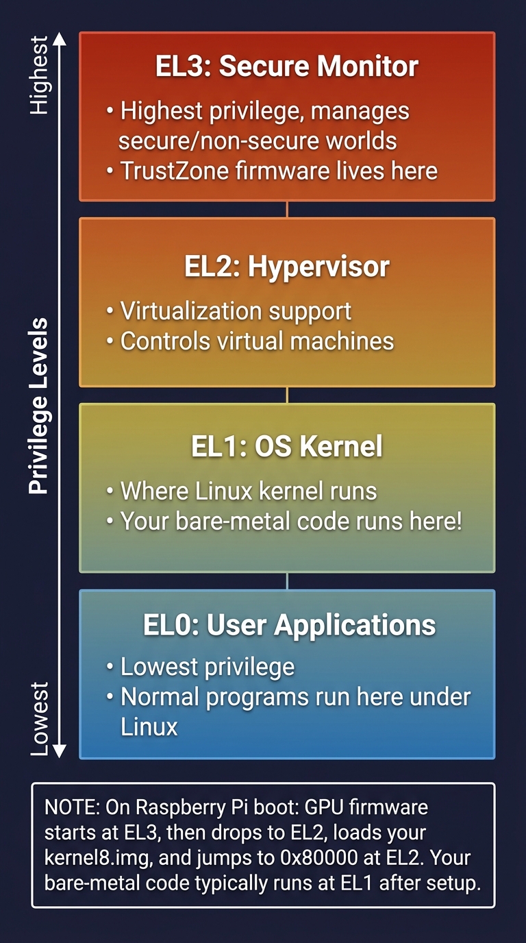
Fundamentals Boot and exception handling define how control flow starts and changes when the system is interrupted. On Cortex-M, reset reads a vector table at a fixed address to obtain the initial stack pointer and reset handler. On AArch64, exception levels (EL0–EL3) define privilege and isolation across kernel, hypervisor, and secure monitor. citeturn0search6turn2search4 Interrupts are structured events with defined entry and exit behavior; when misunderstood, they cause the most common low-level failures (silent lockups, corrupted stacks, and unacknowledged interrupts).
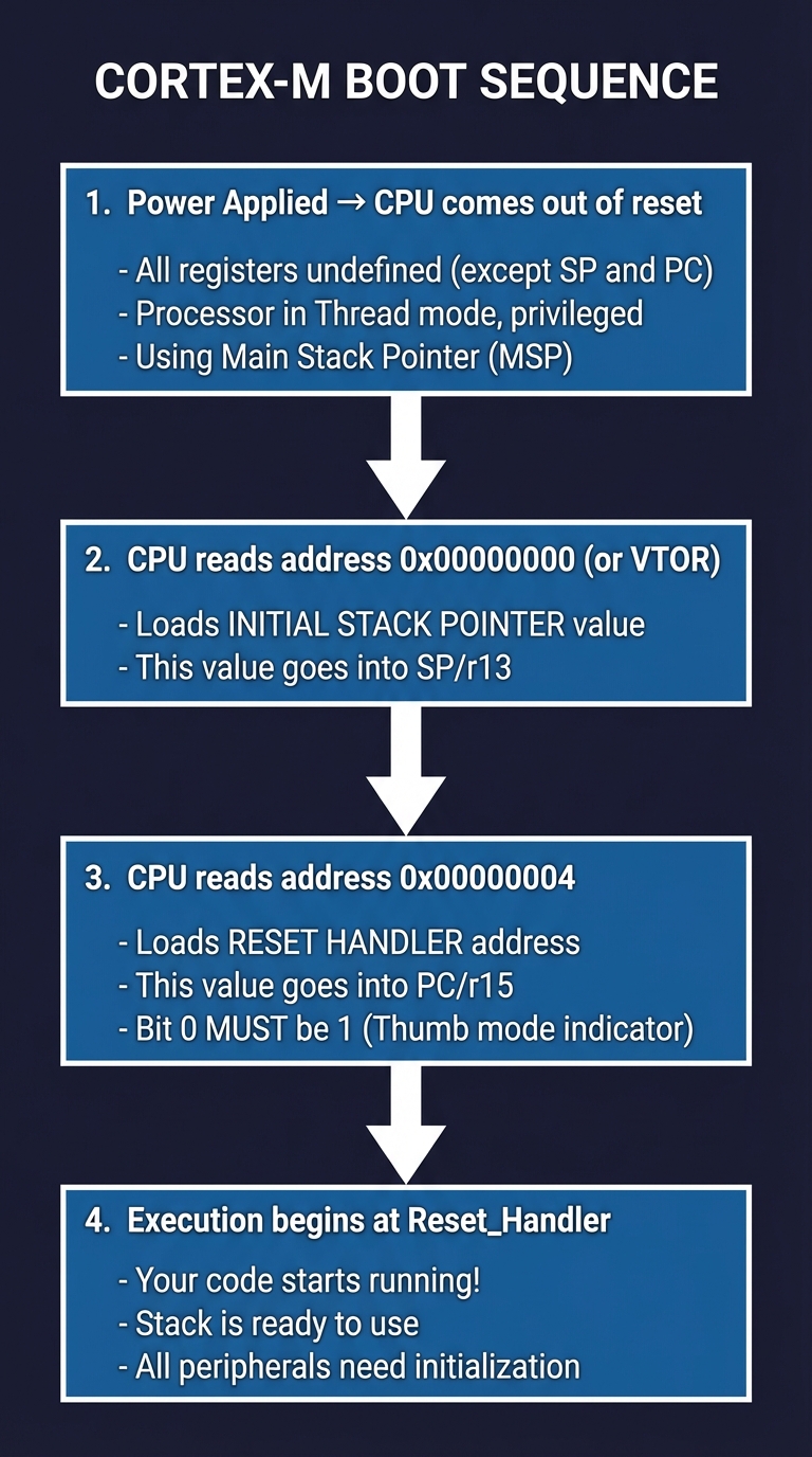
Deep Dive Boot flow is architecture-specific, but it always starts with the hardware choosing a program counter and stack pointer. In Cortex-M, the vector table is a literal list of addresses at the start of flash (or a remapped location). The CPU loads the initial SP from offset 0 and the reset handler from offset 4; execution begins there. This is why vector tables are so critical: a single incorrect address prevents boot. In AArch64 systems, boot is more complex. Firmware (or a ROM) selects the initial exception level and execution state, then transfers control to your image. This can occur at EL2 or EL1 depending on platform; understanding the starting level is essential for setting up the MMU and interrupt controller. citeturn0search6turn2search4
Exceptions and interrupts are structured transitions. On Cortex-M, hardware automatically saves a register frame on the stack and switches to handler mode. This means your ISR is effectively running on a known stack layout; if you violate it, return from interrupt fails. AArch64 exceptions follow a different path: they trap into higher exception levels and use banked registers and exception vector tables that differ per EL. This makes exception handling on A-profile both more powerful and more complex. In practice, you must know which registers are saved by hardware and which you must save manually, and you must understand the difference between synchronous exceptions (e.g., illegal instruction) and asynchronous interrupts (e.g., timer). citeturn0search6turn2search4
Interrupt latency is also a systems-level trade-off. M-profile is designed for low-latency, deterministic responses, which is why it dominates microcontroller workloads. citeturn0search0 This is a critical difference from A-profile, where throughput and virtualization might be prioritized. When you design firmware, you need to decide which tasks are best done in an ISR versus in the main loop; an ISR that does too much can starve other interrupts and introduce jitter.
Finally, exceptions connect directly to debugging. Many “mysterious” crashes are just unhandled faults. On Cortex-M, a hard fault may indicate an invalid memory access or misaligned stack. On AArch64, synchronous exceptions reveal illegal instructions or permission violations. By understanding the exception model, you can interpret fault codes and correlate them to your assembly-level behavior, which is a core skill in systems programming and security analysis.
How this fits on projects
- Central to P05 (Vector Table Builder), P06 (Interrupt-Driven UART), and P07 (Exception Level Lab).
Definitions & key terms
- Vector table: Table of exception handler addresses used at reset or interrupt.
- Exception level: Privilege tier in AArch64 (EL0–EL3). citeturn0search6turn2search4
- ISR: Interrupt service routine.
- HardFault: Cortex-M fault handler for severe errors.
Mental model diagram
Cortex-M Boot Sequence:
━━━━━━━━━━━━━━━━━━━━━━━━━━━━━━━━━━━━━━━━━━━━━━━━━━━━━━━━━━━━━━━━━━━━━━━━

    Power Applied
         │
         ▼
    ┌─────────────────────────────────────────────────────────────────┐
    │  1. CPU comes out of reset                                      │
    │     - All registers undefined (except SP and PC)                │
    │     - Processor in Thread mode, privileged                      │
    │     - Using Main Stack Pointer (MSP)                            │
    └─────────────────────────────────────────────────────────────────┘
         │
         ▼
    ┌─────────────────────────────────────────────────────────────────┐
    │  2. CPU reads address 0x00000000 (or VTOR)                      │
    │     - Loads INITIAL STACK POINTER value                         │
    │     - This value goes into SP/r13                               │
    └─────────────────────────────────────────────────────────────────┘
         │
         ▼
    ┌─────────────────────────────────────────────────────────────────┐
    │  3. CPU reads address 0x00000004                                │
    │     - Loads RESET HANDLER address                               │
    │     - This value goes into PC/r15                               │
    │     - Bit 0 MUST be 1 (Thumb mode indicator)                    │
    └─────────────────────────────────────────────────────────────────┘
         │
         ▼
    ┌─────────────────────────────────────────────────────────────────┐
    │  4. Execution begins at Reset_Handler                           │
    │     - Your code starts running!                                 │
    │     - Stack is ready to use                                     │
    │     - All peripherals need initialization                       │
    └─────────────────────────────────────────────────────────────────┘


Vector Table Structure (first 16 entries are standard Cortex-M):
━━━━━━━━━━━━━━━━━━━━━━━━━━━━━━━━━━━━━━━━━━━━━━━━━━━━━━━━━━━━━━━━━━━━━━━━

    Offset   │  Exception #  │  Contents
    ─────────┼───────────────┼────────────────────────────────────────
    0x0000   │  -            │  Initial Stack Pointer value
    0x0004   │  1 (Reset)    │  Reset_Handler address (| 1 for Thumb)
    0x0008   │  2 (NMI)      │  NMI_Handler address
    0x000C   │  3 (HardFault)│  HardFault_Handler address
    0x0010   │  4            │  Reserved (M0+ doesn't use)
    ...      │  ...          │  ...
    0x003C   │  15 (SysTick) │  SysTick_Handler address
    0x0040   │  16 (IRQ0)    │  First peripheral interrupt
    0x0044   │  17 (IRQ1)    │  Second peripheral interrupt
    ...      │  ...          │  (RP2040 has 26 IRQs)


Example minimal vector table in assembly:
━━━━━━━━━━━━━━━━━━━━━━━━━━━━━━━━━━━━━━━━━━━━━━━━━━━━━━━━━━━━━━━━━━━━━━━━

    .section .vectors, "a"
    .align 2

    .word   _stack_top          // 0x00: Initial SP
    .word   Reset_Handler + 1   // 0x04: Reset (bit 0 = Thumb)
    .word   NMI_Handler + 1     // 0x08: NMI
    .word   HardFault_Handler+1 // 0x0C: HardFault
    .word   0                   // 0x10: Reserved
    // ... more entries ...

NOTE: On RP2040, flash is at 0x10000000, so your vector table
lives there. The boot ROM copies the SP and PC from flash.
AArch64 Exception Levels:
━━━━━━━━━━━━━━━━━━━━━━━━━━━━━━━━━━━━━━━━━━━━━━━━━━━━━━━━━━━━━━━━━━━━━━━━

    ┌─────────────────────────────────────────────────────────────────┐
    │  EL3: Secure Monitor                                            │
    │       - Highest privilege, manages secure/non-secure worlds     │
    │       - TrustZone firmware lives here                           │
    ├─────────────────────────────────────────────────────────────────┤
    │  EL2: Hypervisor                                                │
    │       - Virtualization support                                  │
    │       - Controls virtual machines                               │
    ├─────────────────────────────────────────────────────────────────┤
    │  EL1: OS Kernel                                                 │
    │       - Where Linux kernel runs                                 │
    │       - Your bare-metal code runs here!                         │
    ├─────────────────────────────────────────────────────────────────┤
    │  EL0: User Applications                                         │
    │       - Lowest privilege                                        │
    │       - Normal programs run here under Linux                    │
    └─────────────────────────────────────────────────────────────────┘

    On Raspberry Pi boot:
    ┌──────────────────────────────────────────────────────────────┐
    │ GPU firmware starts at EL3, then drops to EL2,               │
    │ loads your kernel8.img, and jumps to 0x80000 at EL2.         │
    │ Your bare-metal code typically runs at EL1 after setup.      │
    └──────────────────────────────────────────────────────────────┘
Interrupt Flow on Cortex-M:
━━━━━━━━━━━━━━━━━━━━━━━━━━━━━━━━━━━━━━━━━━━━━━━━━━━━━━━━━━━━━━━━━━━━━━━━

    Main Code Running
           │
           │ ← UART receives byte
           │   Hardware sets interrupt flag
           │   NVIC sees enabled interrupt
           ▼
    ┌──────────────────────────────────────────────────────────────────┐
    │  AUTOMATIC HARDWARE ACTIONS (you don't write code for this):    │
    │  1. Finish current instruction                                   │
    │  2. Push 8 registers to stack: r0-r3, r12, LR, PC, xPSR         │
    │  3. Load new PC from vector table (exception #)                  │
    │  4. Load 0xFFFFFFF9 into LR (EXC_RETURN)                        │
    │  5. Enter Handler mode (privileged)                              │
    └──────────────────────────────────────────────────────────────────┘
           │
           ▼
    ┌──────────────────────────────────────────────────────────────────┐
    │  YOUR ISR EXECUTES:                                              │
    │  - Must save r4-r11 if you use them (push {r4-r7})              │
    │  - Read UART data register (clears interrupt flag)               │
    │  - Process byte (store in buffer, set flag, etc.)                │
    │  - Restore r4-r11 if saved                                       │
    │  - Return with: BX LR (the magic EXC_RETURN value)               │
    └──────────────────────────────────────────────────────────────────┘
           │
           ▼
    ┌──────────────────────────────────────────────────────────────────┐
    │  AUTOMATIC HARDWARE ACTIONS:                                     │
    │  1. Hardware detects EXC_RETURN in LR                            │
    │  2. Pop 8 registers from stack                                   │
    │  3. Resume execution exactly where interrupted                   │
    │  4. Return to Thread mode                                        │
    └──────────────────────────────────────────────────────────────────┘
           │
           ▼
    Main Code Continues (unaware anything happened!)


Stack During Interrupt:
━━━━━━━━━━━━━━━━━━━━━━━━━━━━━━━━━━━━━━━━━━━━━━━━━━━━━━━━━━━━━━━━━━━━━━━━

    BEFORE interrupt:           AFTER entry, BEFORE ISR code:
    ┌──────────────┐           ┌──────────────┐
    │  (old data)  │           │  (old data)  │
    │              │           ├──────────────┤
    │              │           │  xPSR        │ ← +0x1C from new SP
    │              │           ├──────────────┤
    │              │           │  PC (return) │ ← +0x18
    │              │           ├──────────────┤
    │              │           │  LR          │ ← +0x14
    │              │           ├──────────────┤
    │              │           │  r12         │ ← +0x10
    │              │           ├──────────────┤
    │              │           │  r3          │ ← +0x0C
    │              │           ├──────────────┤
    │              │           │  r2          │ ← +0x08
    │              │           ├──────────────┤
    │              │           │  r1          │ ← +0x04
    │              │           ├──────────────┤
SP →│              │        SP→│  r0          │ ← +0x00 (new SP)
    └──────────────┘           └──────────────┘

    The 32 bytes (8 × 4) are pushed automatically by hardware!
How it works (step-by-step, with invariants and failure modes)
- Boot loads initial SP and PC from the vector table (Cortex-M) or firmware-defined entry (AArch64). citeturn0search6turn2search4
- An interrupt triggers hardware context save and branches to the handler.
- Handler restores context and returns using the architecture-specific mechanism.
- Failure mode: wrong vector address or corrupted stack → boot hang or fault loop.
Minimal concrete example (pseudo, not runnable)
VECTOR_TABLE[Reset] -> Reset_Handler
On interrupt: push context, branch handler, restore, return
Common misconceptions
- “Interrupt handlers are just normal functions” → They obey different entry/exit rules.
- “Boot is just jump to main” → Boot is a structured sequence with strict alignment rules.
Check-your-understanding questions
- Why must the reset handler address be Thumb-aligned on Cortex-M?
- What does EL1 represent in AArch64?
- Why must ISRs be short?
Check-your-understanding answers
- Bit 0 of the address indicates Thumb state; if it’s wrong, the CPU faults.
- EL1 is the kernel-level privilege where OS code typically runs. citeturn0search6turn2search4
- Long ISRs increase latency and can block higher-priority interrupts.
Real-world applications
- Firmware bootloaders, interrupt-driven I/O, and OS exception handling. citeturn0search0turn0search6
Where you’ll apply it
- P05 Vector Table Builder
- P06 Interrupt-Driven UART
- P07 AArch64 Exception Level Lab
References
- AArch64 exception model and privilege levels. citeturn0search6turn2search4
- Cortex-M profile emphasis on low-latency interrupt response. citeturn0search0
Key insights Boot and exceptions are not features you add later; they are the foundation of control flow.
Summary Once you understand boot and exceptions, most “mysterious” bare-metal failures become obvious.
Homework/Exercises to practice the concept
- Draw the Cortex-M vector table layout and label the first 8 entries.
- Explain how an interrupt differs from a synchronous exception.
Solutions to the homework/exercises
- The first entry is the initial SP, followed by reset, NMI, HardFault, and system handlers.
- Interrupts are asynchronous hardware events; synchronous exceptions are triggered by the current instruction.
Concept 6: Toolchain and Binary Formats (ELF)
Fundamentals Assembly alone is not executable; you need a toolchain to assemble, link, and package code into a binary format. GNU as (the GNU assembler) accepts assembly source and emits object files; the linker combines objects into an executable with sections and symbols. citeturn1search1 On most ARM systems, the object format is ELF, defined by the System V ABI family. citeturn1search4 Understanding sections, symbols, and relocations is essential for boot images, firmware layout, and disassembly.
Deep Dive The toolchain is a pipeline: source → object → linked image. The assembler parses directives, encodes instructions for the target ISA, and emits relocatable objects. The linker then resolves symbols, assigns addresses, applies relocations, and produces a final ELF file or a raw binary. This is not a black box: if your startup code lands at the wrong address or your vector table is misaligned, the linker script is responsible. The GNU assembler manual documents directive syntax and how the assembler handles sections, alignment, and symbols. citeturn1search1
ELF (Executable and Linkable Format) is the standard container for compiled objects. It defines headers, sections, and symbol tables so tools can reason about what is in a binary. citeturn1search4 ELF’s strength is transparency: you can inspect sections such as .text (code), .data (initialized data), .bss (zero-initialized data), and custom sections for vector tables or boot metadata. In embedded contexts, you often convert ELF into a raw binary that can be flashed, but the ELF remains the authoritative artifact for debugging because it contains symbols and relocation information.
Relocations are where everything connects. When the assembler emits an instruction that references a symbol whose address is not yet known, it emits a relocation entry. The linker later resolves it. This is how references to labels, functions, and global variables are patched. If you understand relocations, you can interpret why certain instructions appear in disassembly, and you can identify errors like “relocation overflow” or “undefined reference.” The same reasoning applies to position-independent code or shared libraries on A-profile systems.
In practical terms, mastering the toolchain lets you answer questions like: Why is my vector table not at the start of flash? Why does the linker place my .data in RAM but my .text in flash? Why does a symbol show up as undefined? These are the exact questions you will encounter in bare-metal ARM development, and they can only be solved by understanding ELF and the linker. The toolchain also connects to diagnostics: objdump and readelf are not just utilities; they are the microscope that lets you see what the assembler and linker actually produced.
How this fits on projects
- Core to P01 (Toolchain Pipeline Explorer) and P10 (Capstone Monitor).
Definitions & key terms
- Assembler: Translates assembly source into object files. citeturn1search1
- Linker: Resolves symbols and produces an executable or binary.
- ELF: Executable and Linkable Format for binaries. citeturn1search4
- Relocation: A placeholder that the linker resolves to a final address.
Mental model diagram
Toolchain Flow
──────────────
Source (.s) → Assembler → Object (.o) → Linker → ELF (.elf) → Binary (.bin)
                    │                 │
               Symbols/Relocs    Sections/Addresses
How it works (step-by-step, with invariants and failure modes)
- Assemble source into relocatable objects.
- Link with a linker script or default layout.
- Verify ELF sections and symbols.
- Failure mode: wrong section placement → boot hangs or interrupts jump to wrong address.
Minimal concrete example (pseudo, not runnable)
.section .vectors
.word reset_handler
.linker: place .vectors at flash start
Common misconceptions
- “ELF is only for OS programs” → It is central in embedded, too. citeturn1search4
- “Linker script is optional” → Not when you need precise memory layout.
Check-your-understanding questions
- What is the role of a relocation entry?
- Why do embedded projects often convert ELF to raw binary?
- What is the difference between
.textand.bss?
Check-your-understanding answers
- It records a reference the linker must patch with a final address.
- Flashing tools often want raw bytes, but ELF holds symbols for debugging.
.textholds code;.bssholds zero-initialized data.
Real-world applications
- Firmware image layout, boot loaders, and disassembly tooling.
Where you’ll apply it
- P01 Toolchain Pipeline Explorer
- P10 Capstone Monitor
References
- GNU assembler manual. citeturn1search1
- ELF format and ABI overview. citeturn1search4
Key insights The toolchain is the bridge between assembly and hardware; without it, nothing runs.
Summary Understanding ELF and linking turns build failures into solvable layout problems.
Homework/Exercises to practice the concept
- Identify three sections you expect in a bare-metal ELF and explain why.
- Explain how a symbol reference becomes a concrete address.
Solutions to the homework/exercises
.textfor code,.datafor initialized globals,.bssfor zeroed globals.- The assembler emits a relocation that the linker resolves to the final address.
Glossary
- AArch64: 64-bit execution state for ARMv8-A.
- ABI: Application Binary Interface; rules for calling and binary layout.
- ELF: Executable and Linkable Format.
- MMIO: Memory-mapped I/O; addresses that control hardware.
- Vector table: Table of exception handler addresses used by the CPU.
Why ARM Assembly Matters
- Modern motivation: ARM is the dominant architecture for mobile and embedded systems, and it is rapidly expanding in servers and cloud workloads.
- Real-world statistics: Arm reported ~7 billion Arm-based chips shipped in the quarter ending March 31, 2024, with a cumulative total of 287+ billion chips shipped. citeturn4search2
- Impact: Reuters (2023) reports Arm-based CPUs power about 99% of smartphones, underscoring why ARM expertise maps to the dominant mobile ecosystem. citeturn4search3
Old Model (Black Box)               New Model (Assembly-Aware)
┌──────────────────────────┐        ┌──────────────────────────┐
│ High-level language only │        │ Knows registers & MMIO   │
│ "Why did this fail?"     │   →    │ "Which register spilled?"│
│                          │        │ "Which barrier missing?" │
└──────────────────────────┘        └──────────────────────────┘
Context & Evolution
- ARM evolved from embedded efficiency into a broad computing ecosystem; profiles and execution states reflect that expansion. citeturn0search0turn0search1turn0search2
Concept Summary Table
| Concept Cluster | What You Need to Internalize |
|---|---|
| Profiles & Execution States | A/M/R profiles and AArch64/AArch32/Thumb states define which instructions and system features are valid. |
| Registers & Calling Convention | Register roles, stack behavior, and ABI rules are mandatory for correct control flow. |
| Instruction Encoding | Encodings explain operand limits, instruction size, and why some sequences require expansion. |
| Memory & Ordering | MMIO semantics and barriers determine when devices see your writes. |
| Boot & Exceptions | Vector tables and exception levels define how control flow begins and changes. |
| Toolchain & ELF | Assemblers and linkers turn text into runnable binaries with explicit memory layout. |
Project-to-Concept Map
| Project | Concepts Applied |
|---|---|
| Project 1 | Profiles & Execution States, Toolchain & ELF |
| Project 2 | Registers & Calling Convention |
| Project 3 | Instruction Encoding |
| Project 4 | Memory & Ordering |
| Project 5 | Boot & Exceptions, Toolchain & ELF |
| Project 6 | Boot & Exceptions, Memory & Ordering |
| Project 7 | Profiles & Execution States, Boot & Exceptions |
| Project 8 | Registers & Calling Convention |
| Project 9 | Memory & Ordering |
| Project 10 | Toolchain & ELF, Boot & Exceptions |
Deep Dive Reading by Concept
| Concept | Book and Chapter | Why This Matters |
|---|---|---|
| Profiles & Execution States | “Computer Organization and Design: ARM Edition” - Ch. 1-2 | ISA and architecture context. |
| Registers & Calling Convention | “ARM Assembly Language” by William Hohl - Ch. 3-4 | Register usage and calling patterns. |
| Instruction Encoding | “ARM Assembly Language” by William Hohl - Ch. 5 | Encoding constraints and instruction forms. |
| Memory & Ordering | “The Definitive Guide to ARM Cortex-M3/M4” by Joseph Yiu - Ch. 4-6 | Memory map and peripheral access. |
| Boot & Exceptions | “The Definitive Guide to ARM Cortex-M3/M4” by Joseph Yiu - Ch. 10-12 | Exception handling and vector tables. |
| Toolchain & ELF | “Linkers and Loaders” by John R. Levine - Ch. 1-3 | Sections, symbols, and relocations. |
Quick Start
Day 1:
- Read Concept 1 and Concept 2 in the Theory Primer.
- Start Project 1 and produce the first toolchain artifacts.
Day 2:
- Validate Project 1 against the Definition of Done.
- Read Concept 3 and sketch the Thumb encoding diagram by hand.
Recommended Learning Paths
Path 1: The Embedded Builder
- Project 1 → Project 3 → Project 4 → Project 5 → Project 6 → Project 10
Path 2: The Systems Engineer
- Project 1 → Project 2 → Project 7 → Project 8 → Project 9 → Project 10
Success Metrics
- You can explain why a specific instruction encoding fails without trial-and-error.
- You can trace an interrupt from hardware event to handler and back.
- You can inspect an ELF and explain where code and data live.
Tooling & Debugging Appendix
Toolchain Cheat Sheet (No code, just intent)
as: assemble text into object files. citeturn1search1ld: link object files into ELF images.objdump: inspect instructions and sections.readelf: inspect ELF headers and symbols. citeturn1search4
Project Overview Table
| # | Project Name | Main Language | Difficulty | Time Estimate | Core Concepts | Coolness |
|---|---|---|---|---|---|---|
| 1 | Toolchain Pipeline Explorer | Assembly + C | Level 2 | 6-10 hrs | Profiles, ELF | ★★★☆☆ |
| 2 | Register & Stack Visualizer | Assembly + C | Level 2 | 8-12 hrs | Registers, ABI | ★★★☆☆ |
| 3 | Thumb Encoder/Decoder | Python/C | Level 3 | 10-16 hrs | Encoding | ★★★★☆ |
| 4 | Memory Map & MMIO Notebook | Assembly + C | Level 3 | 10-16 hrs | MMIO, Ordering | ★★★☆☆ |
| 5 | Vector Table Builder | Assembly | Level 3 | 12-18 hrs | Boot, Exceptions | ★★★☆☆ |
| 6 | Interrupt-Driven UART Echo | Assembly + C | Level 4 | 16-24 hrs | Interrupts, MMIO | ★★★★☆ |
| 7 | AArch64 Exception Lab | Assembly + C | Level 4 | 16-24 hrs | ELs, Boot | ★★★★☆ |
| 8 | ABI Conformance Audit | Python | Level 3 | 10-14 hrs | ABI, Registers | ★★★☆☆ |
| 9 | Memory Ordering Litmus | C | Level 4 | 16-24 hrs | Barriers, Ordering | ★★★★☆ |
| 10 | Capstone Hardware Monitor | Assembly + C | Level 5 | 30-40 hrs | All | ★★★★★ |
Project List
The following projects guide you from toolchain fluency to full bare-metal reasoning.
Project 1: Toolchain Pipeline Explorer
- File: P01-toolchain-pipeline-explorer.md
- Main Programming Language: ARM Assembly + C
- Alternative Programming Languages: Rust, Zig
- Coolness Level: Level 2 (See REFERENCE.md)
- Business Potential: Level 2 (See REFERENCE.md)
- Difficulty: Level 2 (See REFERENCE.md)
- Knowledge Area: Toolchains, Binary Formats
- Software or Tool: GNU binutils, objdump, readelf
- Main Book: “Linkers and Loaders” by John R. Levine
What you will build: A repeatable pipeline that assembles, links, and inspects both Cortex-M and AArch64 binaries.
Why it teaches ARM assembly: You will observe how the same assembly intent produces different encodings and ELF layouts across execution states.
Core challenges you will face:
- Target selection -> Profiles & Execution States
- Section layout -> Toolchain & ELF
- Binary inspection -> Instruction Encoding
Real World Outcome
You can generate and inspect a minimal ELF for both targets and explain the role of each section.
CLI output (example):
$ arm-toolchain-lab --target cortex-m0 --show-sections
ELF: sample.elf
.text  @ 0x10000000  size 0x120
.vectors @ 0x10000000 size 0x40
.bss   @ 0x20000000  size 0x80

$ arm-toolchain-lab --target aarch64 --show-sections
ELF: sample.elf
.text  @ 0x00080000  size 0x180
.rodata @ 0x00082000 size 0x40
.bss   @ 0x00100000  size 0x100
The Core Question You Are Answering
“How do assembly source files become concrete bytes in memory, and how does that differ across ARM execution states?”
This reveals the precise place where intent becomes machine reality: the assembler and linker.
Concepts You Must Understand First
- Profiles & Execution States
- What does AArch64 vs Thumb mean for encoding and sections?
- Book Reference: “Computer Organization and Design: ARM Edition” - Ch. 1-2
- Toolchain & ELF
- What does an ELF section represent?
- Book Reference: “Linkers and Loaders” - Ch. 1-3
Questions to Guide Your Design
- Binary Layout
- How will you verify where
.textand.vectorsare placed? - How will you ensure the correct entry point for each target?
- How will you verify where
- Verification Strategy
- Which tool will you trust to inspect sections and symbols?
- How will you compare two binaries for encoding differences?
Thinking Exercise
Trace the Pipeline
Draw the path from source to flash and label where errors can occur.
Questions to answer:
- Where does a label become an address?
- What happens if two sections overlap in the linker script?
The Interview Questions They Will Ask
- “What is the difference between an object file and an ELF executable?”
- “Why do embedded projects use linker scripts?”
- “What is a relocation entry?”
- “How do you verify your vector table is at the correct address?”
- “Why would the same assembly source produce different binaries on AArch64 and Thumb?”
Hints in Layers
Hint 1: Start with just one section
Use a single .text section and verify its address before adding .vectors or .bss.
Hint 2: Compare disassembly, not source Focus on the machine code bytes to see how encodings differ.
Hint 3: Inspect symbols
Dump the symbol table and ensure _start and reset handlers resolve correctly.
Hint 4: Validate layout Use an ELF inspector to confirm section order and addresses.
Books That Will Help
| Topic | Book | Chapter |
|---|---|---|
| Linking and layout | “Linkers and Loaders” by John R. Levine | Ch. 1-3 |
| ARM ISA context | “Computer Organization and Design: ARM Edition” | Ch. 1-2 |
Common Pitfalls and Debugging
Problem 1: “Binary boots on one target but not the other”
- Why: Wrong execution state or entry point.
- Fix: Verify target triple and entry symbol.
- Quick test: Inspect ELF header and entry address.
Definition of Done
- ELF sections are correctly placed for both targets
- Entry points match the expected reset or start address
- Disassembly matches expected encoding class (Thumb vs A64)
- Results are reproducible across builds
Project 2: Register & Stack Visualizer
- File: P02-register-stack-visualizer.md
- Main Programming Language: ARM Assembly + C
- Alternative Programming Languages: Rust
- Coolness Level: Level 3 (See REFERENCE.md)
- Business Potential: Level 1 (See REFERENCE.md)
- Difficulty: Level 2 (See REFERENCE.md)
- Knowledge Area: Calling Conventions, Debugging
- Software or Tool: GDB, QEMU or hardware debugger
- Main Book: “ARM Assembly Language” by William Hohl
What you will build: A small program that logs register and stack changes across a chain of function calls.
Why it teaches ARM assembly: You will see the ABI rules in action as registers and stack frames evolve.
Core challenges you will face:
- Register preservation -> Registers & Calling Conventions
- Stack alignment -> Registers & Calling Conventions
- Call/return flow -> Toolchain & ELF
Real World Outcome
You can run a trace and see a step-by-step log of register values and stack pointer changes.
$ regstack-trace --target aarch64 --depth 3
CALL depth=1  SP=0x0000000000107ff0  LR=0x0000000000080120
CALL depth=2  SP=0x0000000000107fd0  LR=0x0000000000080154
CALL depth=3  SP=0x0000000000107fb0  LR=0x0000000000080188
RETURN depth=3 SP=0x0000000000107fd0
RETURN depth=2 SP=0x0000000000107ff0
RETURN depth=1 SP=0x0000000000108000
The Core Question You Are Answering
“What does a function call actually do to registers and the stack on ARM?”
Concepts You Must Understand First
- Registers & Calling Convention
- Which registers must be preserved?
- Book Reference: “ARM Assembly Language” - Ch. 3-4
- Toolchain & ELF
- How do you read symbols for function addresses?
- Book Reference: “Linkers and Loaders” - Ch. 1-2
Questions to Guide Your Design
- Trace Design
- Which registers will you log at entry and exit?
- How will you avoid disturbing the state you are measuring?
- Output Format
- How will you ensure output is comparable across runs?
- How will you include the call depth clearly?
Thinking Exercise
Draw a Stack Frame
Sketch the stack before and after a call and label which values must be preserved.
Questions to answer:
- Which register holds the return address on your target?
- What is the alignment requirement at call boundaries?
The Interview Questions They Will Ask
- “What is the role of the link register?”
- “What is the difference between caller-saved and callee-saved registers?”
- “Why must the stack be aligned?”
- “How can you verify a function preserved its registers?”
- “Why do AArch64 and Cortex-M have different register usage patterns?”
Hints in Layers
Hint 1: Start with entry/exit markers Log just SP and LR at function entry/exit before logging anything else.
Hint 2: Preserve the state Use a scratch buffer so your logging doesn’t overwrite registers you want to observe.
Hint 3: Compare against ABI rules Check whether callee-saved registers are unchanged across calls.
Hint 4: Validate with a debugger Use single-step debugging to confirm the trace is accurate.
Books That Will Help
| Topic | Book | Chapter |
|---|---|---|
| Register usage | “ARM Assembly Language” by William Hohl | Ch. 3-4 |
| ABI basics | “Linkers and Loaders” by John R. Levine | Ch. 1 |
Common Pitfalls and Debugging
Problem 1: “Trace output changes when logging is enabled”
- Why: Logging perturbs registers and stack.
- Fix: Save/restore any registers you touch for logging.
- Quick test: Compare trace with and without logging.
Definition of Done
- Stack pointer changes are consistent with call depth
- Callee-saved registers are preserved
- Trace output is deterministic
- You can explain each line in the trace
Project 3: Thumb Instruction Encoder/Decoder
- File: P03-thumb-encoder-decoder.md
- Main Programming Language: Python or C
- Alternative Programming Languages: Rust, Go
- Coolness Level: Level 4 (See REFERENCE.md)
- Business Potential: Level 2 (See REFERENCE.md)
- Difficulty: Level 3 (See REFERENCE.md)
- Knowledge Area: Instruction Encoding
- Software or Tool: Reference manuals, hex dump tools
- Main Book: “ARM Assembly Language” by William Hohl
What you will build: A small tool that converts between a subset of Thumb mnemonics and machine-code bit patterns.
Why it teaches ARM assembly: Encoding forces you to understand the exact bit layout of instructions.
Core challenges you will face:
- Bitfield packing -> Instruction Encoding
- Immediate range limits -> Instruction Encoding
- Endianness -> Instruction Encoding
Real World Outcome
You can enter a mnemonic and see its exact 16-bit encoding (and vice versa).
$ thumb-encode "MOV r0, #42"
encoding: 0b00100 000 00101010
hex: 0x202A

$ thumb-decode 0xE000
B label (unconditional branch)
The Core Question You Are Answering
“How do mnemonic fields become concrete bits, and what constraints do they impose?”
Concepts You Must Understand First
- Instruction Encoding
- What are the bit fields for registers and immediates?
- Book Reference: “ARM Assembly Language” - Ch. 5
- Profiles & Execution States
- Why does Thumb encoding differ from A64?
- Book Reference: “Computer Organization and Design: ARM Edition” - Ch. 1
Questions to Guide Your Design
- Instruction Subset
- Which 6-8 instructions are most representative of encoding patterns?
- How will you handle invalid patterns?
- Round-trip Tests
- How will you verify encode→decode→encode consistency?
- What is your error format for unsupported inputs?
Thinking Exercise
Bitfield Sketching
Draw the bit layout for a single Thumb MOV and label each field.
Questions to answer:
- Which bits represent the destination register?
- What is the maximum immediate size for this encoding?
The Interview Questions They Will Ask
- “Why does Thumb use 16-bit encodings?”
- “What happens if an immediate doesn’t fit?”
- “How does little-endian affect instruction bytes?”
- “How would you detect an illegal opcode?”
- “Why is decoding state-dependent?”
Hints in Layers
Hint 1: Encode one instruction first Implement MOV or ADD before tackling branches.
Hint 2: Represent bitfields explicitly Use a table of field positions and widths.
Hint 3: Add decode tests Verify that known hex values decode to expected mnemonics.
Hint 4: Handle errors early Return a clear error when a field overflows.
Books That Will Help
| Topic | Book | Chapter |
|---|---|---|
| Instruction encoding | “ARM Assembly Language” by William Hohl | Ch. 5 |
| ISA overview | “Computer Organization and Design: ARM Edition” | Ch. 1 |
Common Pitfalls and Debugging
Problem 1: “Decoder outputs nonsense”
- Why: Mixing endianness or wrong execution state.
- Fix: Normalize byte order and confirm Thumb context.
- Quick test: Decode known reference instructions.
Definition of Done
- Encodes at least 6 Thumb instructions accurately
- Decodes known hex sequences correctly
- Round-trip tests pass
- Error handling is explicit and documented
Project 4: Memory Map & MMIO Field Notebook
- File: P04-mmio-memory-map-notebook.md
- Main Programming Language: ARM Assembly + C
- Alternative Programming Languages: Rust
- Coolness Level: Level 3 (See REFERENCE.md)
- Business Potential: Level 2 (See REFERENCE.md)
- Difficulty: Level 3 (See REFERENCE.md)
- Knowledge Area: MMIO, Hardware Interfaces
- Software or Tool: Datasheets, emulator or hardware
- Main Book: “The Definitive Guide to ARM Cortex-M3/M4” by Joseph Yiu
What you will build: A documented MMIO reference and a small tool to compute register addresses and bitfields.
Why it teaches ARM assembly: You will translate raw addresses into meaningful hardware behavior.
Core challenges you will face:
- Address calculation -> Memory Maps & MMIO
- Atomic register semantics -> Memory Maps & MMIO
- Ordering requirements -> Memory Ordering
Real World Outcome
You can query a register by name and get its address, fields, and access rules.
$ mmio-notebook lookup GPIO_OUT_SET
Base: 0xD0000000
Offset: 0x014
Address: 0xD0000014
Access: write-only
Behavior: atomically sets GPIO output bits
The Core Question You Are Answering
“What exactly happens when I read or write a peripheral address?”
Concepts You Must Understand First
- Memory Maps & MMIO
- Why are peripherals mapped into address space?
- Book Reference: “The Definitive Guide to ARM Cortex-M3/M4” - Ch. 4-6
- Memory Ordering
- When do you need barriers?
- Book Reference: “Computer Architecture: A Quantitative Approach” - Ch. 5
Questions to Guide Your Design
- Data Model
- How will you represent base addresses, offsets, and bitfields?
- How will you encode read-only vs write-only semantics?
- Validation
- How will you verify that computed addresses match the datasheet?
- What does a mismatch imply?
Thinking Exercise
Map a Peripheral
Pick UART and manually compute its data and status register addresses.
Questions to answer:
- Which offsets are read-only vs write-only?
- Which registers must be accessed atomically?
The Interview Questions They Will Ask
- “What is memory-mapped I/O and why is it used?”
- “Why can a read from a register change hardware state?”
- “How do you avoid read-modify-write races?”
- “When do you need a memory barrier for device access?”
- “What is the difference between MMIO and normal RAM?”
Hints in Layers
Hint 1: Start with one peripheral Build the notebook for just GPIO first.
Hint 2: Encode access rules Track read/write/clear-on-read semantics explicitly.
Hint 3: Compare to a known map Cross-check one register with a second source (datasheet or SDK).
Hint 4: Add ordering notes Annotate where barriers are required.
Books That Will Help
| Topic | Book | Chapter |
|---|---|---|
| MMIO fundamentals | “The Definitive Guide to ARM Cortex-M3/M4” | Ch. 4-6 |
| Memory systems | “Computer Architecture: A Quantitative Approach” | Ch. 5 |
Common Pitfalls and Debugging
Problem 1: “Writes appear to do nothing”
- Why: Wrong address or missing clock enable.
- Fix: Verify base address and peripheral enable sequence.
- Quick test: Read a status register to confirm peripheral state.
Definition of Done
- Notebook includes at least 3 peripherals with full address maps
- Access rules are documented (R/W/RO/WO)
- Atomic vs non-atomic registers are identified
- Computed addresses match datasheet values
Project 5: Vector Table Builder
- File: P05-vector-table-builder.md
- Main Programming Language: ARM Assembly
- Alternative Programming Languages: C, Rust
- Coolness Level: Level 3 (See REFERENCE.md)
- Business Potential: Level 1 (See REFERENCE.md)
- Difficulty: Level 3 (See REFERENCE.md)
- Knowledge Area: Boot, Exceptions
- Software or Tool: Linker scripts, hex viewer
- Main Book: “The Definitive Guide to ARM Cortex-M3/M4” by Joseph Yiu
What you will build: A correct Cortex-M vector table and reset sequence that reliably boots on an emulator or hardware.
Why it teaches ARM assembly: Boot is the first test of correct encoding, layout, and system understanding.
Core challenges you will face:
- Vector layout -> Boot & Exceptions
- Alignment -> Toolchain & ELF
- Reset handler flow -> Registers & Calling Conventions
Real World Outcome
A boot image that prints a recognizable startup banner and does not hard-fault.
$ bootlab-run --board pico
[BOOT] Vector table OK
[BOOT] Reset handler entered
[BOOT] Stack initialized at 0x20041000
The Core Question You Are Answering
“What exactly must exist at address 0x00000000 for a Cortex-M to boot?”
Concepts You Must Understand First
- Boot & Exceptions
- What is in the vector table?
- Book Reference: “The Definitive Guide to ARM Cortex-M3/M4” - Ch. 10-12
- Toolchain & ELF
- How do you place sections at fixed addresses?
- Book Reference: “Linkers and Loaders” - Ch. 2
Questions to Guide Your Design
- Vector Table Placement
- How will you ensure the table is at the correct address?
- How do you verify alignment?
- Reset Handler
- What minimal initialization must occur before C code?
- How do you confirm the handler is in Thumb state?
Thinking Exercise
Vector Layout Check
Write down the first eight vector entries and their meaning.
Questions to answer:
- Why does the reset handler address have bit 0 set?
- Which entry corresponds to SysTick?
The Interview Questions They Will Ask
- “What is a vector table?”
- “Why must the reset handler be Thumb-aligned?”
- “What happens if the stack pointer is wrong at reset?”
- “How do you place a section at a fixed address?”
- “What causes a HardFault on boot?”
Hints in Layers
Hint 1: Start with a minimal table Only include initial SP and reset handler before adding other vectors.
Hint 2: Verify section placement
Confirm the .vectors section address in the ELF.
Hint 3: Add a known pattern Place a recognizable constant in flash to confirm mapping.
Hint 4: Use a debugger Check SP and PC immediately after reset.
Books That Will Help
| Topic | Book | Chapter |
|---|---|---|
| Boot sequence | “The Definitive Guide to ARM Cortex-M3/M4” | Ch. 10-12 |
| Linking | “Linkers and Loaders” | Ch. 2 |
Common Pitfalls and Debugging
Problem 1: “Boot loops or hard-faults immediately”
- Why: Vector table at wrong address or invalid reset handler.
- Fix: Verify the vector table section placement and alignment.
- Quick test: Inspect first 8 words of flash.
Definition of Done
- Vector table placed at correct flash address
- Reset handler runs and outputs a banner
- SP initialized to valid RAM
- No HardFault on startup
Project 6: Interrupt-Driven UART Echo
- File: P06-interrupt-driven-uart-echo.md
- Main Programming Language: ARM Assembly + C
- Alternative Programming Languages: Rust
- Coolness Level: Level 4 (See REFERENCE.md)
- Business Potential: Level 2 (See REFERENCE.md)
- Difficulty: Level 4 (See REFERENCE.md)
- Knowledge Area: Interrupts, MMIO
- Software or Tool: UART, debugger
- Main Book: “The Definitive Guide to ARM Cortex-M3/M4” by Joseph Yiu
What you will build: An interrupt-driven UART echo loop on Cortex-M that uses an ISR to capture bytes.
Why it teaches ARM assembly: It combines MMIO, vector tables, and interrupt context preservation.
Core challenges you will face:
- ISR correctness -> Boot & Exceptions
- Register preservation -> Registers & Calling Conventions
- MMIO access -> Memory Maps & MMIO
Real World Outcome
Typing into the UART console returns each character via ISR-based echo.
$ uart-echo
> hello
hello
> arm
arm
The Core Question You Are Answering
“How does hardware preempt my code and return safely after servicing an interrupt?”
Concepts You Must Understand First
- Boot & Exceptions
- How are interrupt handlers located?
- Book Reference: “The Definitive Guide to ARM Cortex-M3/M4” - Ch. 10-12
- Memory Maps & MMIO
- Which UART registers must be read to clear interrupts?
- Book Reference: “The Definitive Guide to ARM Cortex-M3/M4” - Ch. 6
Questions to Guide Your Design
- Interrupt Entry/Exit
- Which registers are automatically saved by hardware?
- Which must you preserve manually?
- UART Behavior
- What clears the RX interrupt flag?
- How will you avoid buffer overruns?
Thinking Exercise
Interrupt Timeline
Draw a timeline showing when the UART interrupt fires and when it is cleared.
Questions to answer:
- What happens if you do not read the data register?
- How long can the ISR run before losing bytes?
The Interview Questions They Will Ask
- “How does Cortex-M save state on interrupt entry?”
- “Why must ISRs be short?”
- “How do you acknowledge a UART interrupt?”
- “What is EXC_RETURN?”
- “How do you prevent nested interrupts from corrupting state?”
Hints in Layers
Hint 1: Start with polling Verify UART by polling before switching to interrupts.
Hint 2: Keep ISR minimal Only read the byte and store it; process later in main loop.
Hint 3: Validate vector table Confirm the UART handler address in the vector table.
Hint 4: Use a ring buffer Prevent data loss by buffering bytes quickly.
Books That Will Help
| Topic | Book | Chapter |
|---|---|---|
| Interrupt handling | “The Definitive Guide to ARM Cortex-M3/M4” | Ch. 10-12 |
| UART basics | “Embedded Systems” by Jonathan Valvano | Ch. 7 |
Common Pitfalls and Debugging
Problem 1: “ISR triggers once, then never again”
- Why: Interrupt flag not cleared.
- Fix: Read the UART data register to clear the flag.
- Quick test: Inspect interrupt status register after ISR.
Definition of Done
- UART echo works with interrupts enabled
- ISR preserves required registers
- No data loss at typical baud rates
- Interrupt flags are cleared correctly
Project 7: AArch64 Exception Level Lab
- File: P07-aarch64-exception-level-lab.md
- Main Programming Language: ARM Assembly + C
- Alternative Programming Languages: Rust
- Coolness Level: Level 4 (See REFERENCE.md)
- Business Potential: Level 3 (See REFERENCE.md)
- Difficulty: Level 4 (See REFERENCE.md)
- Knowledge Area: Privilege Levels, Boot
- Software or Tool: Raspberry Pi or QEMU
- Main Book: “Armv8-A Architecture Reference Manual” (spec)
What you will build: A minimal lab that reports current exception level and transitions to EL1.
Why it teaches ARM assembly: It exposes the privilege model and system register setup for A-profile systems. citeturn0search6turn2search4
Core challenges you will face:
- Execution state handling -> Profiles & Execution States
- Exception model -> Boot & Exceptions
- System register setup -> Toolchain & ELF
Real World Outcome
You can boot and print a trace of exception level transitions.
$ aarch64-el-lab
EL at entry: EL2
Configured EL1 state
Dropped to EL1
EL now: EL1
The Core Question You Are Answering
“What privilege level am I running in, and how do I safely change it?”
Concepts You Must Understand First
- Profiles & Execution States
- What is AArch64, and why does it matter here?
- Book Reference: “Computer Organization and Design: ARM Edition” - Ch. 1
- Boot & Exceptions
- What do EL0–EL3 represent?
- Book Reference: “Armv8-A Architecture Reference Manual” - Exception model chapters
Questions to Guide Your Design
- State Transition
- Which registers control target EL and state?
- How will you verify the transition succeeded?
- Diagnostics
- How will you report errors if the transition fails?
- What is your fallback if the system traps unexpectedly?
Thinking Exercise
Exception Path
Draw the path from EL2 to EL1 and mark which register changes are required.
Questions to answer:
- Which exception vector is used at EL2?
- How do you prevent re-entry into EL2?
The Interview Questions They Will Ask
- “What are the four exception levels in AArch64?”
- “Why do some platforms boot at EL2?”
- “What happens if you execute privileged instructions at EL0?”
- “How do you set the stack pointer for EL1?”
- “Why is exception level management critical for OS bring-up?”
Hints in Layers
Hint 1: Read the current EL Start by reporting the current exception level without changing it.
Hint 2: Use a minimal transition Only set the required registers for EL1 and keep the rest default.
Hint 3: Confirm with a trace Print the EL before and after the transition.
Hint 4: Watch for traps If you land in an exception handler unexpectedly, log the syndrome register.
Books That Will Help
| Topic | Book | Chapter |
|---|---|---|
| Exception levels | “Armv8-A Architecture Reference Manual” | Exception model |
| AArch64 boot | “ARM 64-Bit Assembly Language” by Larry Pyeatt | Ch. 9 |
Common Pitfalls and Debugging
Problem 1: “System hangs immediately after transition”
- Why: Stack pointer not set for the target EL.
- Fix: Initialize SP for EL1 before the transition.
- Quick test: Print EL and SP registers before and after.
Definition of Done
- Current EL is correctly reported
- Transition to EL1 succeeds
- No unexpected exceptions occur
- Output log is deterministic
Project 8: ABI Conformance Audit
- File: P08-abi-conformance-audit.md
- Main Programming Language: Python
- Alternative Programming Languages: Rust, Go
- Coolness Level: Level 3 (See REFERENCE.md)
- Business Potential: Level 3 (See REFERENCE.md)
- Difficulty: Level 3 (See REFERENCE.md)
- Knowledge Area: ABI, Disassembly
- Software or Tool: objdump, readelf
- Main Book: “ARM Assembly Language” by William Hohl
What you will build: A static checker that inspects compiled functions for ABI compliance.
Why it teaches ARM assembly: You will read real instruction sequences and verify calling convention rules. citeturn3search7
Core challenges you will face:
- Register classification -> Registers & Calling Conventions
- Stack alignment -> Registers & Calling Conventions
- Function boundaries -> Toolchain & ELF
Real World Outcome
You can analyze a binary and flag ABI violations with clear explanations.
$ abi-audit sample.elf
OK: function foo preserves x19-x20
WARN: function bar modifies x19 without saving
OK: stack aligned to 16 bytes at call sites
The Core Question You Are Answering
“Does this compiled code obey the ABI rules required for safe interop?”
Concepts You Must Understand First
- Registers & Calling Convention
- Which registers are callee-saved in AAPCS64?
- Book Reference: “ARM Assembly Language” - Ch. 3-4
- Toolchain & ELF
- How do you identify function boundaries in a binary?
- Book Reference: “Linkers and Loaders” - Ch. 1
Questions to Guide Your Design
- Function Identification
- Will you use symbol tables or pattern heuristics?
- How will you handle stripped binaries?
- Rule Enforcement
- Which ABI rules will you enforce first?
- How will you report violations?
Thinking Exercise
ABI Checklist
Write a checklist of rules you expect every function to obey.
Questions to answer:
- Which registers must never be clobbered?
- How can you detect stack misalignment from disassembly?
The Interview Questions They Will Ask
- “What is the AAPCS64 and why does it matter?”
- “Which registers are callee-saved?”
- “How can you detect a missing stack frame?”
- “Why can ABI violations cause random crashes?”
- “What does it mean for a function to be leaf?”
Hints in Layers
Hint 1: Use symbol tables first Start with binaries that contain symbols.
Hint 2: Track prologue/epilogue patterns Look for standard stack frame setup and teardown.
Hint 3: Flag only high-confidence violations Avoid false positives by requiring clear evidence.
Hint 4: Provide explanations Show which rule was violated and where.
Books That Will Help
| Topic | Book | Chapter |
|---|---|---|
| Calling conventions | “ARM Assembly Language” by William Hohl | Ch. 3-4 |
| Binary structure | “Linkers and Loaders” | Ch. 1 |
Common Pitfalls and Debugging
Problem 1: “Too many false positives”
- Why: Incomplete function boundary detection.
- Fix: Require symbol support or implement a stronger heuristic.
- Quick test: Validate against a known-good binary.
Definition of Done
- Detects at least two categories of ABI violations
- Produces clear, deterministic reports
- Handles binaries with symbols correctly
- Documents limitations (e.g., stripped binaries)
Project 9: Memory Ordering Litmus Tests
- File: P09-memory-ordering-litmus.md
- Main Programming Language: C
- Alternative Programming Languages: Rust
- Coolness Level: Level 4 (See REFERENCE.md)
- Business Potential: Level 2 (See REFERENCE.md)
- Difficulty: Level 4 (See REFERENCE.md)
- Knowledge Area: Concurrency, Memory Ordering
- Software or Tool: QEMU or multi-core hardware
- Main Book: “Computer Architecture: A Quantitative Approach” by Hennessy & Patterson
What you will build: A small suite of litmus tests that demonstrate ordering anomalies and barrier fixes.
Why it teaches ARM assembly: You will see how DMB/DSB/ISB change observable behavior. citeturn3search3
Core challenges you will face:
- Reordering effects -> Memory Ordering
- Barrier placement -> Memory Ordering
- Deterministic reporting -> Toolchain & ELF
Real World Outcome
You can run a test and observe reordering cases disappear when barriers are added.
$ ordering-test --case store-buffering
Observed outcomes (100000 runs):
  0,0  -> 42
  0,1  -> 55231
  1,0  -> 44727
  1,1  -> 0
After adding DMB:
  0,0  -> 0
The Core Question You Are Answering
“Why does correct-looking code fail on weakly ordered systems, and how do barriers fix it?”
Concepts You Must Understand First
- Memory Ordering
- What do DMB/DSB/ISB guarantee?
- Book Reference: “Computer Architecture: A Quantitative Approach” - Ch. 5
- Toolchain & ELF
- How do you ensure consistent builds for reproducible tests?
- Book Reference: “Linkers and Loaders” - Ch. 1
Questions to Guide Your Design
- Test Design
- Which litmus cases are representative (store buffering, load buffering)?
- How will you capture and count outcomes?
- Barrier Placement
- Where exactly should barriers be inserted?
- How will you show the difference before/after?
Thinking Exercise
Reordering Scenario
Draw two cores writing and reading shared variables without barriers.
Questions to answer:
- Which outcome is unexpected?
- What would a barrier change?
The Interview Questions They Will Ask
- “What does a memory barrier guarantee?”
- “Why can two cores see writes in different orders?”
- “What is the difference between DMB and DSB?”
- “Why are litmus tests useful?”
- “How do you make concurrency tests deterministic?”
Hints in Layers
Hint 1: Start with a known litmus test Implement store-buffering first.
Hint 2: Fix the measurement Use a fixed number of iterations and report counts deterministically.
Hint 3: Add one barrier at a time Show the smallest change that eliminates the anomaly.
Hint 4: Confirm on two targets Run in QEMU and on hardware if possible.
Books That Will Help
| Topic | Book | Chapter |
|---|---|---|
| Memory ordering | “Computer Architecture: A Quantitative Approach” | Ch. 5 |
| Concurrency | “Operating Systems: Three Easy Pieces” | Ch. 28 |
Common Pitfalls and Debugging
Problem 1: “Results are inconsistent between runs”
- Why: Non-deterministic scheduling and timing.
- Fix: Fix iteration counts and seed any randomness.
- Quick test: Run with a single fixed CPU frequency.
Definition of Done
- At least two litmus tests implemented
- Barrier effects are observable and documented
- Output is deterministic across runs
- Explanation of results is clear
Project 10: Capstone Hardware Monitor
- File: P10-capstone-hardware-monitor.md
- Main Programming Language: ARM Assembly + C
- Alternative Programming Languages: Rust
- Coolness Level: Level 5 (See REFERENCE.md)
- Business Potential: Level 4 (See REFERENCE.md)
- Difficulty: Level 5 (See REFERENCE.md)
- Knowledge Area: Systems Integration
- Software or Tool: UART, timers, debugger
- Main Book: “The Definitive Guide to ARM Cortex-M3/M4” by Joseph Yiu
What you will build: A bare-metal hardware monitor that boots, initializes UART, handles interrupts, and exposes a minimal command interface.
Why it teaches ARM assembly: It forces you to combine every concept into a working system with observable outputs.
Core challenges you will face:
- Boot + Vector table -> Boot & Exceptions
- MMIO control -> Memory Maps & MMIO
- Toolchain layout -> Toolchain & ELF
Real World Outcome
A bootable monitor that accepts simple commands and reports hardware state.
$ monitor
[BOOT] OK
> regs
SP=0x20041000 LR=0x10000124
> mmio GPIO_OUT
0x00000020
> help
commands: regs, mmio, echo, reboot
The Core Question You Are Answering
“Can I build a minimal, reliable ARM system from scratch without an OS?”
Concepts You Must Understand First
- Boot & Exceptions
- How does the system start and handle interrupts?
- Book Reference: “The Definitive Guide to ARM Cortex-M3/M4” - Ch. 10-12
- Memory Maps & MMIO
- How do you read and write peripheral registers safely?
- Book Reference: “The Definitive Guide to ARM Cortex-M3/M4” - Ch. 4-6
- Toolchain & ELF
- How do you place code and data precisely?
- Book Reference: “Linkers and Loaders” - Ch. 2
Questions to Guide Your Design
- Command Interface
- How will you parse commands without dynamic memory?
- How will you handle unknown commands?
- System Initialization
- What is the minimum init sequence for UART and timers?
- How will you confirm correct clock setup?
Thinking Exercise
Boot-to-Command Flow
Draw the exact sequence from reset to first prompt.
Questions to answer:
- Which step depends on MMIO ordering?
- Which step depends on vector table correctness?
The Interview Questions They Will Ask
- “How do you bring up a bare-metal system?”
- “What are the first three registers you check on boot?”
- “How do you handle input without an OS?”
- “How do you debug a boot hang?”
- “What does a minimal monitor need to be useful?”
Hints in Layers
Hint 1: Start with a boot banner Only print a startup line before adding commands.
Hint 2: Add one command at a time
Implement regs, then mmio, then echo.
Hint 3: Keep state explicit Store command buffers in a fixed memory region.
Hint 4: Validate with a debugger Break at reset and confirm SP and PC.
Books That Will Help
| Topic | Book | Chapter |
|---|---|---|
| Bare-metal bring-up | “The Definitive Guide to ARM Cortex-M3/M4” | Ch. 10-12 |
| Memory maps | “The Definitive Guide to ARM Cortex-M3/M4” | Ch. 4-6 |
| Linking | “Linkers and Loaders” | Ch. 2 |
Common Pitfalls and Debugging
Problem 1: “Boot banner never appears”
- Why: Vector table misplacement or UART not initialized.
- Fix: Verify reset handler and UART registers.
- Quick test: Toggle a GPIO pin in the reset handler.
Definition of Done
- Boot banner prints reliably
- UART commands operate deterministically
- MMIO reads/writes are correct and documented
- System survives repeated resets
Project Comparison Table
| Project | Difficulty | Time | Depth of Understanding | Fun Factor |
|---|---|---|---|---|
| 1. Toolchain Pipeline Explorer | Level 2 | Weekend | Medium | ★★★☆☆ |
| 2. Register & Stack Visualizer | Level 2 | Weekend | Medium | ★★★☆☆ |
| 3. Thumb Encoder/Decoder | Level 3 | 1-2 weeks | High | ★★★★☆ |
| 4. Memory Map & MMIO Notebook | Level 3 | 1-2 weeks | High | ★★★☆☆ |
| 5. Vector Table Builder | Level 3 | 1-2 weeks | High | ★★★☆☆ |
| 6. Interrupt-Driven UART Echo | Level 4 | 2-3 weeks | High | ★★★★☆ |
| 7. AArch64 Exception Lab | Level 4 | 2-3 weeks | High | ★★★★☆ |
| 8. ABI Conformance Audit | Level 3 | 1-2 weeks | Medium | ★★★☆☆ |
| 9. Memory Ordering Litmus | Level 4 | 2-3 weeks | High | ★★★★☆ |
| 10. Capstone Hardware Monitor | Level 5 | 1 month | Very High | ★★★★★ |
Recommendation
If you are new to ARM assembly: Start with Project 1 to demystify the toolchain and binary layout. If you are an embedded developer: Start with Project 4 to anchor your understanding in MMIO and memory maps. If you want OS-level systems skills: Start with Project 7 to master exception levels and privilege transitions.
Final Overall Project: Unified ARM Bring-Up Suite
The Goal: Combine Projects 1, 5, 6, and 10 into a unified bring-up suite that can boot, initialize peripherals, and expose a diagnostic console.
- Build a validated toolchain pipeline (Project 1).
- Generate a correct vector table and reset flow (Project 5).
- Add interrupt-driven UART and timer events (Project 6).
- Expand into a minimal monitor (Project 10).
Success Criteria: The system boots reliably, prints a banner, and responds to at least three commands without faults.
From Learning to Production: What Is Next
| Your Project | Production Equivalent | Gap to Fill |
|---|---|---|
| Toolchain Pipeline Explorer | Firmware build system | CI reproducibility, vendor integration |
| Vector Table Builder | Bootloader | Secure boot, update strategy |
| Interrupt-Driven UART | Device driver | Power management, robustness testing |
| Capstone Monitor | Embedded firmware shell | Security hardening, diagnostics |
Summary
This learning path covers ARM assembly through 10 hands-on projects.
| # | Project Name | Main Language | Difficulty | Time Estimate |
|---|---|---|---|---|
| 1 | Toolchain Pipeline Explorer | Assembly + C | Level 2 | 6-10 hrs |
| 2 | Register & Stack Visualizer | Assembly + C | Level 2 | 8-12 hrs |
| 3 | Thumb Encoder/Decoder | Python/C | Level 3 | 10-16 hrs |
| 4 | Memory Map & MMIO Notebook | Assembly + C | Level 3 | 10-16 hrs |
| 5 | Vector Table Builder | Assembly | Level 3 | 12-18 hrs |
| 6 | Interrupt-Driven UART Echo | Assembly + C | Level 4 | 16-24 hrs |
| 7 | AArch64 Exception Lab | Assembly + C | Level 4 | 16-24 hrs |
| 8 | ABI Conformance Audit | Python | Level 3 | 10-14 hrs |
| 9 | Memory Ordering Litmus | C | Level 4 | 16-24 hrs |
| 10 | Capstone Hardware Monitor | Assembly + C | Level 5 | 30-40 hrs |
Expected Outcomes
- You can inspect an ELF and explain its layout.
- You can reason about register state across calls and interrupts.
- You can build a minimal ARM system from reset to I/O.
Additional Resources and References
Standards and Specifications
- Arm A-profile architecture overview (execution states). citeturn0search2
- AAPCS64 procedure call standard repository. citeturn3search7
- ELF format and ABI overview. citeturn1search4
Industry Analysis
- Arm SEC filing on cumulative chip shipments (2024). citeturn4search2
- Reuters on Arm’s smartphone CPU share. citeturn4search3
Books
- “ARM Assembly Language” by William Hohl - practical assembly patterns.
- “The Definitive Guide to ARM Cortex-M3/M4” by Joseph Yiu - boot and interrupts.
- “Linkers and Loaders” by John R. Levine - ELF and linking.